Rainbow Electronics MAX711 User Manual
Page 2
MAX710/MAX711
3.3V/5V or Adjustable,
Step-Up/Down DC-DC Converters
2
_______________________________________________________________________________________
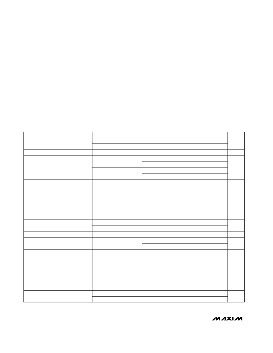
ABSOLUTE MAXIMUM RATINGS
ELECTRICAL CHARACTERISTICS
(V
PS
= 5.6V,
STBY = PS, C
REF
= 0.1µF, C
OUT
= 4.7µF, T
A
= -40°C to +85°C, unless otherwise noted. Typical values are at
T
A
= +25°C.) (Note 1)
Stresses beyond those listed under “Absolute Maximum Ratings” may cause permanent damage to the device. These are stress ratings only, and functional
operation of the device at these or any other conditions beyond those indicated in the operational sections of the specifications is not implied. Exposure to
absolute maximum rating conditions for extended periods may affect device reliability.
PS, LX, OUT to GND............................................-0.3V to +11.5V
ILIM, SHDN, STBY, FB, 3/5, N/E, LBO,
LBI-, LBI+, REF to GND ...........................-0.3V to (V
PS
+ 0.3V)
PGND to GND .......................................................-0.3V to +0.3V
REF Short Circuit to GND ...........................................Continuous
I
OUT
...................................................................................700mA
Continuous Power Dissipation (T
A
= +70°C)
SO (derate 8.70mW/°C above +70°C) ..........................696mW
Operating Temperature Range ...........................-40°C to +85°C
Storage Temperature Range .............................-65°C to +160°C
Junction Temperature ......................................................+150°C
Lead Temperature (soldering, 10sec) .............................+300°C
ILIM = GND
ILIM = PS
V
LX
= 5.6V
MAX711, V
PS
= 2.7V
MAX710, V
PS
= 3.7V
V
STBY
= 0V, linear regulator
V
PS
= 5.6V
FB = 1.25V
T
A
= -40°C to +85°C, I
REF
= 0
T
A
= 0°C to +85°C, I
REF
= 0
MAX711
V
STBY
= V
SHDN
= logic high, current measured
into PS pin; I
LOAD
= 0
V
STBY
= 0V
V
SHDN
= 0V
MAX711, OUT = FB
CONDITIONS
A
1.1
1.5
1.95
LX Current Limit
0.5
0.8
1.3
µA
0.1
1
LX Leakage Current
Ω
0.6
1.2
LX On-Resistance
0.3
0.9
0.2
0.6
nA
1
50
FB Input Current
mV
1.18
1.25
1.31
FB Voltage
V
0.9
Full Load Start-Up Voltage
1.20
1.25
1.29
mA
10
Standby Output Current
V
1.23
1.28
1.32
Reference Voltage
1.24
1.28
1.31
V
FB
5.5
Output Voltage-Adjustment Range
µA
100
140
Quiescent Current
µA
7
16
Standby Quiescent Current
µA
0.1
5
Shutdown Quiescent Current
UNITS
MIN
TYP
MAX
PARAMETER
T
A
= 0°C to +85°C
T
A
= -40°C to +85°C
0mA
≤
I
LOAD
≤
250mA
MAX711, OUT = FB
%
0.1
1
Load Regulation
3/5 = low,
I
OUT
= 0 to 250mA
V
4.8
5.0
5.2
T
A
= 0°C to +85°C
4.6
5.0
5.3
T
A
= -40°C to +85°C
3/5 = high, I
OUT
= 0 to
250mA, V
PS
= 4.7V
3.17
3.3
3.43
T
A
= 0°C to +85°C
3.05
3.3
3.55
T
A
= -40°C to +85°C
Output Voltage (MAX710)
0 < I
OUT
< 250mA, STBY = PS
%
0.5
Output Voltage Load Regulation
STBY = PS, 1.8V to 5V
%/V
0.3
Output Voltage Line Regulation
N/E = GND (Note 2)
N/E = PS
V
1.8
7.0
1.8
11.0
Input Voltage