Pin description, Getting started, Detailed description – Rainbow Electronics MAX746 User Manual
Page 6
MAX746
High-Efficiency, PWM, Step-Down,
N-Channel DC-DC Controller
6
_______________________________________________________________________________________
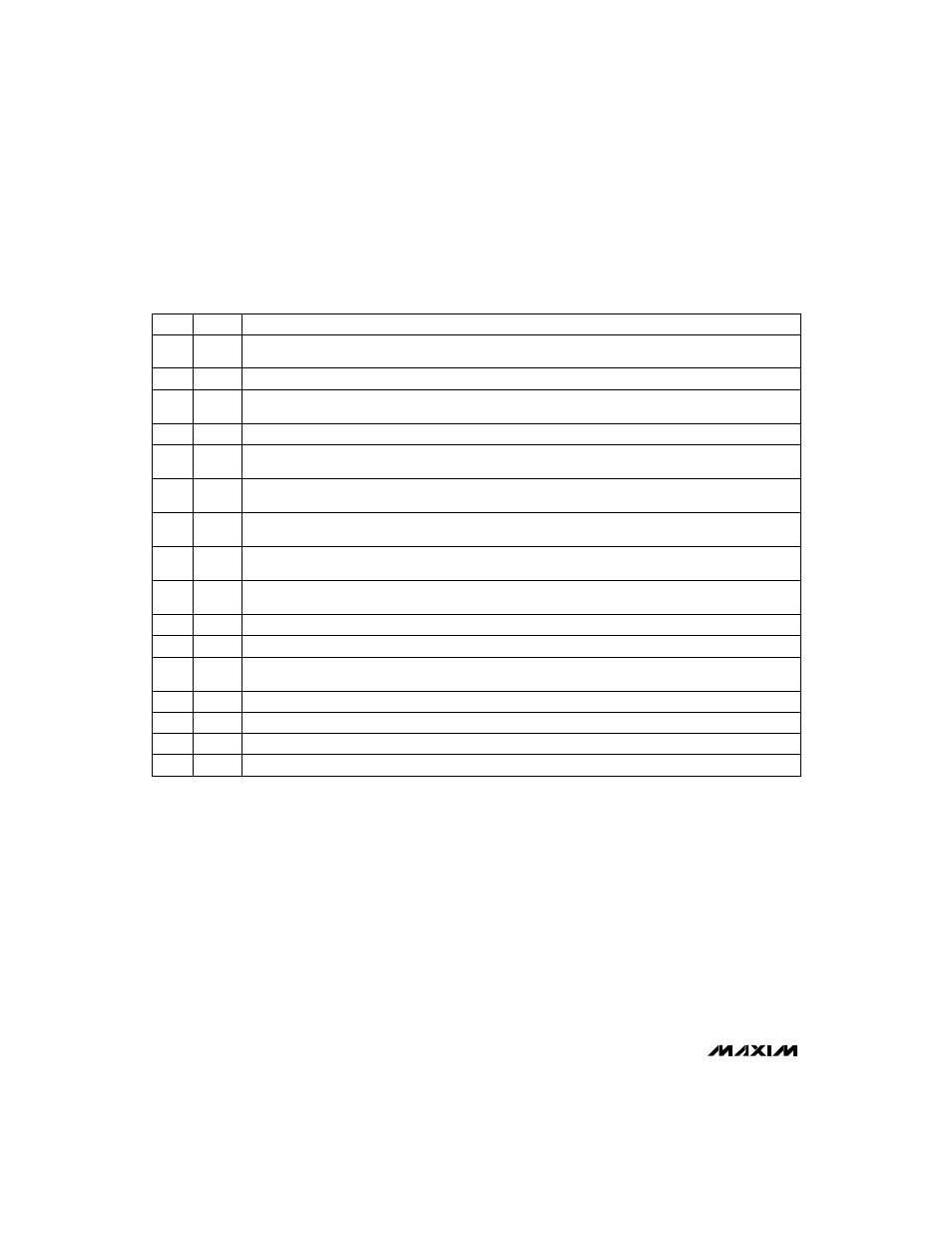
______________________________________________________________Pin Description
PIN
NAME
FUNCTION
1
LBO
3
SS
4
REF
5
SHDN
6
FB
7
CC
8
AV+
9
OUT
10
CS
11
AGND
Quiet analog ground.
12
EXT
13
HIGH
Regulated high-side voltage, 5V above the V+ supply voltage.
14
CP
Charge-pump output that generates a 0V to V+, 50kHz square wave (see
Charge Pump
section).
15
V+
High-current supply voltage for the charge pump.
Low-battery output is an open-drain output that goes low when LBI is less than 2V. Connect to V+ through a
pull-up resistor. Leave floating if not used. LBO is disabled in shutdown mode.
Soft-start limits start-up surge currents. On power-up, it charges the soft-start capacitor, slowly raising the peak
current limit to the level set by the sense resistor.
2V reference output can source 100
µ
A for external loads. Bypass with 1
µ
F. The reference is disabled in shutdown mode.
Active-high logic input. In shutdown mode, V
OUT
= 0V and the supply current is reduced to less than 20
µ
A.
Connect to GND for normal operation.
Feedback input for adjustable-output operation. Connect to GND for fixed 5V output. Use a resistor-divider net-
work to adjust the output voltage (see
Setting the Output Voltage
section).
AC compensation input for the error amplifier. Connect a capacitor between CC and GND for fixed 5V-output
operation (see
Compensation Capacitor
section).
Quiet supply voltage for sensitive analog circuitry. Also the noninverting input to the current-sense amplifier. A
separate bypass capacitor is not recommended for AV+.
Output voltage sense that connects to the internal resistor divider. Bypass with 0.1
µ
F to AGND, close to the IC
for fixed output operation. Leave unconnected for adjustable-output operation.
Inverting input to the current-sense amplifier. Connect the current-sense resistor (R
SENSE
) from AV+ to CS.
Power MOSFET gate-drive output that swings between HIGH and GND. EXT is not protected against short cir-
cuits to V+ or AGND.
16
GND
High-current ground return for the output driver and charge pump.
____________________Getting Started
Figure 1a shows the 5V-output 3A standard application
circuit, Figure 1b shows the 3.3V-output 3A standard
application circuit, and Figure 1c shows the 5V-output
1.5A standard application circuit. Most applications will
be served by these circuits. To learn more about compo-
nent selection for particular applications, refer to the
Design Procedure section. To learn more about the oper-
ation of the MAX746, refer to the
Detailed Description.
_______________Detailed Description
The MAX746 monolithic, CMOS, step-down, switch-
mode power-supply controller provides high-side drive
for external logic-level N-channel FETs. A charge pump
generates a voltage 5V above the supply voltage for
high-side drive capability. The MAX746 uses a unique
current-mode pulse-width-modulating (PWM) control
scheme that results in tight output-voltage regulation,
excellent load- and line-transient response, low noise,
and high efficiency over a wide range of load currents.
Efficiency at light loads is further enhanced by a propri-
etary idle-mode switching control scheme that skips
oscillator cycles in order to reduce switching losses.
Other features include undervoltage lockout, shutdown,
and a low-battery detection comparator.
Operating Principle
Figure 2 is the MAX746 block diagram. The MAX746
regulates using an inner current-feedback loop and an
outer voltage-feedback loop. A slope-compensation
scheme stabilizes the current loop; the dominant pole,
formed by the output filter capacitor and the load,
stabilizes the voltage loop.
2
LBI
Input to the low-battery comparator. Tie to V+ or GND if not used.