Rainbow Electronics MAX1243 User Manual
Page 7
MAX1242/MAX1243
+2.7V to +5.25V, Low-Power, 10-Bit
Serial ADCs in SO-8
_______________________________________________________________________________________
7
AIN
TRACK INPUT
HOLD
GND
TRACK
HOLD
9k
R
IN
C
HOLD
16pF
-
+
C
SWITCH
COMPARATOR
ZERO
REF
CAPACITIVE DAC
AT THE SAMPLING INSTANT,
THE INPUT SWITCHES FROM
AIN TO GND.
SHUTDOWN
INPUT
ANALOG INPUT
0V TO V
REF
+2.7V to +5.25V
1
2
3
4
V
DD
AIN
SHDN
REF
8
7
6
5
SCLK
CS
DOUT
GND
SERIAL
INTERFACE
C*
*4.7
µ
F, MAX1242
0.1
µ
F, MAX1243
4.7
µ
F 0.1
µ
F
REFERENCE
INPUT
MAX1243
MAX1242
MAX1243
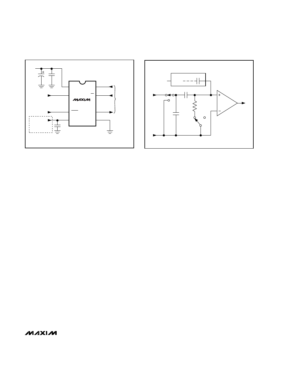
Figure 3. Operational Diagram
Figure 4. Equivalent Input Circuit
where R
IN
= 9k
Ω
, R
S
= the input signal’s source imped-
ance, and t
ACQ
is never less than 1.5µs. Source imped-
ances below 4k
Ω
do not significantly affect the ADC’s
AC performance.
Higher source impedances can be used if a 0.01µF
capacitor is connected to the analog input. Note that
the input capacitor forms an RC filter with the input
source impedance, limiting the ADC’s input signal
bandwidth.
Input Bandwidth
The ADC’s input tracking circuitry has a 2.25MHz
small-signal bandwidth, so it is possible to digitize
high-speed transient events and measure periodic sig-
nals with bandwidths exceeding the ADC’s sampling
rate by using undersampling techniques. To avoid
aliasing of unwanted high-frequency signals into the
frequency band of interest, anti-alias filtering is recom-
mended.
Analog Input Protection
Internal protection diodes, which clamp the analog
input to V
DD
and GND, allow the input to swing from
GND - 0.3V to V
DD
+ 0.3V without damage. However,
for accurate conversions near full scale, the input must
not exceed V
DD
by more than 50mV, or be lower than
GND by 50mV.
If the analog input exceeds 50mV beyond the supplies,
limit the input current to 2mA.
Internal Reference (MAX1242)
The MAX1242 has an on-chip voltage reference
trimmed to 2.5V. The internal reference output is con-
nected to REF and also drives the internal capacitive
DAC. The output can be used as a reference voltage
source for other components and can source up to
400µA. Bypass REF with a 4.7µF capacitor. Larger
capacitors increase wake-up time when exiting shut-
down (see
Using
SHDN to Reduce Supply Current
).
The internal reference is enabled by pulling the SHDN
pin high. Letting SHDN float disables the internal refer-
ence, which allows the use of an external reference, as
described in the
External Reference
section.
External Reference
The MAX1242/MAX1243 operate with an external refer-
ence at the REF pin. To use the MAX1242 with an
external reference, disable the internal reference by let-
ting SHDN float. Stay within the voltage range 1.0V to
V
DD
to achieve specified accuracy. The minimum input
impedance is 18k
Ω
for DC currents. During conver-
sion, the external reference must be able to deliver up
to 250µA of DC load current and have an output
impedance of 10
Ω
or less. The recommended mini-
mum value for the bypass capacitor is 0.1µF. If the ref-
erence has higher output impedance or is noisy,
bypass it close to the REF pin with a 4.7µF capacitor.