Shift register mode timing waveforms, Float waveforms (1), At89lv55 – Rainbow Electronics AT89LV55 User Manual
Page 21: Float waveforms
AT89LV55
21
Serial Port Timing: Shift Register Mode Test Conditions
The values in this table are valid for V
CC
= 5.0V
± 20% and Load Capacitance = 80 pF.
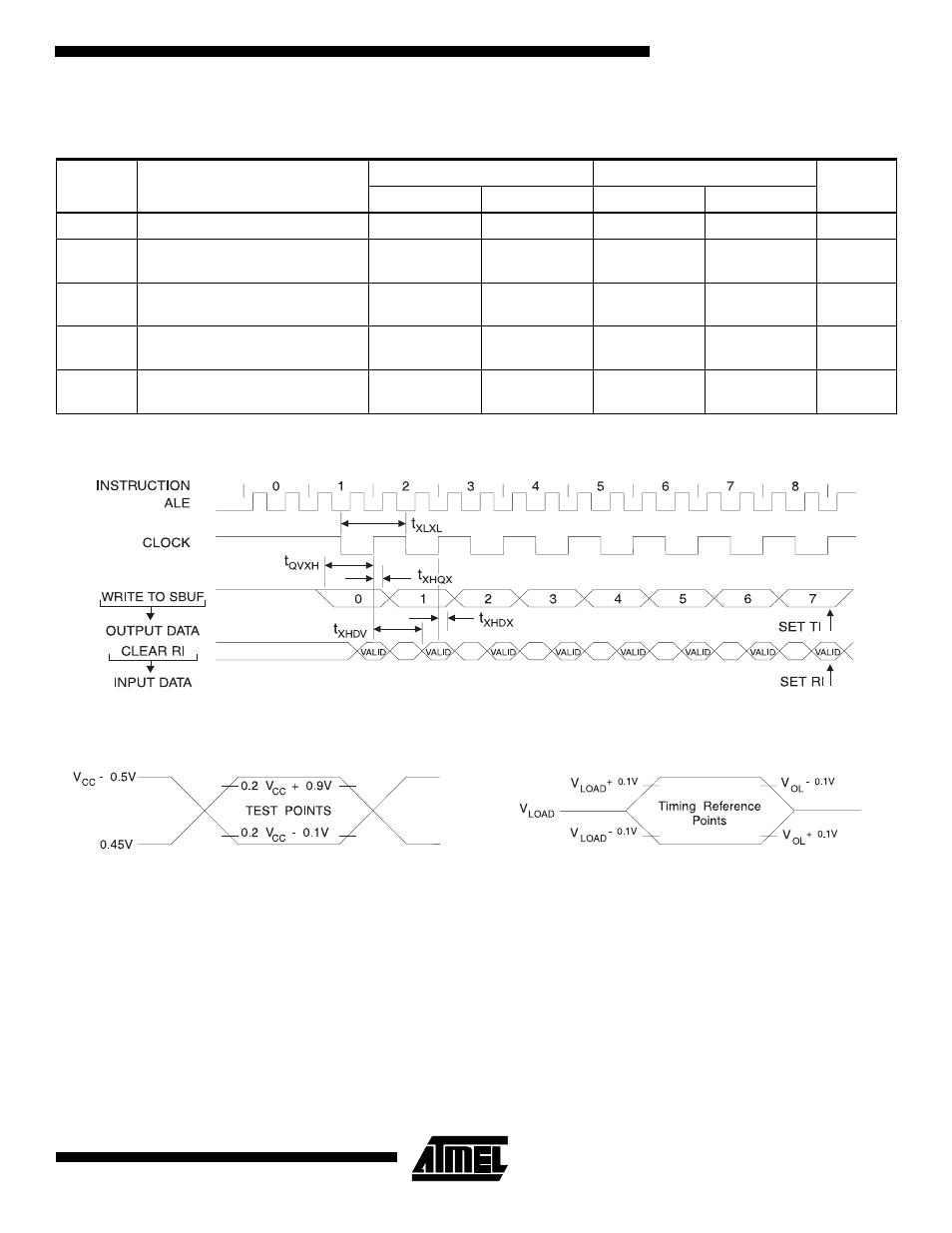
Shift Register Mode Timing Waveforms
AC Testing Input/Output Waveforms
Note:
1.
AC Inputs during testing are driven at 2.4V for a
logic “1” and 0.45V for a logic “0”. Timing measure-
ments are made at 2.0V for a logic “1” and 0.8V for a
logic “0”.
Float Waveforms
Note:
1.
For timing purposes, a port pin is no longer floating
when a 100 mV change from load voltage occurs. A
port pin begins to float when a 100 mV change from
the loaded V
OH
/V
OL
level occurs.
Symbol
Parameter
12 MHz Osc
Variable Oscillator
Units
Min
Max
Min
Max
t
XLXL
Serial Port Clock Cycle Time
1.0
12t
CLCL
ns
t
QVXH
Output Data Setup to Clock Rising
Edge
700
10t
CLCL
- 133
ns
t
XHQX
Output Data Hold After Clock
Rising Edge
50
2t
CLCL
- 117
ns
t
XHDX
Input Data Hold After Clock Rising
Edge
0
0
ns
t
XHDV
Clock Rising Edge to Input Data
Valid
700
10t
CLCL
- 133
ns