Dc characteristics, At89lv55, Absolute maximum ratings* dc characteristics – Rainbow Electronics AT89LV55 User Manual
Page 17
AT89LV55
17
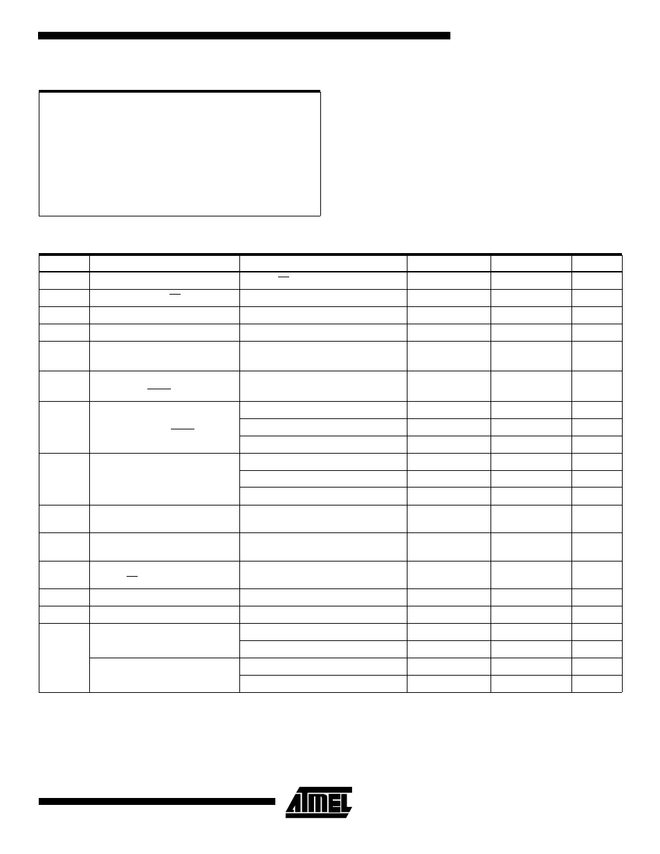
Absolute Maximum Ratings*
DC Characteristics
The values shown in this table are valid for T
A
= -40°C to 85°C and V
CC
= 2.7V to 6.0V, unless otherwise noted.
Notes:
1. Under steady state (non-transient) conditions, I
OL
must be externally limited as follows:
Maximum I
OL
per port pin: 10 mA
Maximum I
OL
per 8-bit port:
Port 0: 26 mA, Ports 1, 2, 3: 15 mA
Maximum total I
OL
for all output pins: 71 mA
If I
OL
exceeds the test condition, V
OL
may exceed the
related specification. Pins are not guaranteed to sink
current greater than the listed test conditions.
2. Minimum V
CC
for Power Down is 2V.
Operating Temperature ................................. -55°C to +125°C
*NOTICE:
Stresses beyond those listed under “Absolute
Maximum Ratings” may cause permanent dam-
age to the device. This is a stress rating only and
functional operation of the device at these or any
other conditions beyond those indicated in the
operational sections of this specification is not
implied. Exposure to absolute maximum rating
conditions for extended periods may affect device
reliability.
Storage Temperature ..................................... -65°C to +150°C
Voltage on Any Pin
with Respect to Ground .....................................-1.0V to +7.0V
Maximum Operating Voltage ............................................ 6.6V
DC Output Current...................................................... 15.0 mA
Symbol
Parameter
Condition
Min
Max
Units
V
IL
Input Low Voltage
(Except EA)
-0.5
0.2 V
CC
- 0.1
V
V
IL1
Input Low Voltage (EA)
-0.5
0.2 V
CC
- 0.3
V
V
IH
Input High Voltage
(Except XTAL1, RST)
0.2 V
CC
+ 0.9
V
CC
+ 0.5
V
V
IH1
Input High Voltage
(XTAL1, RST)
0.7 V
CC
V
CC
+ 0.5
V
V
OL
Output Low Voltage
(Ports 1, 2, 3)
I
OL
= 1.6 mA
0.45
V
V
OL1
Output Low Voltage
(Port 0, ALE, PSEN)
I
OL
= 3.2 mA
0.45
V
V
OH
Output High Voltage
(Ports 1, 2, 3, ALE, PSEN)
I
OH
= -60
µA, V
CC
= 5V
± 10%
2.4
V
I
OH
= -25
µA
0.75 V
CC
V
I
OH
= -10
µA
0.9 V
CC
V
V
OH1
Output High Voltage
(Port 0 in External Bus Mode)
I
OH
= -800
µA, V
CC
= 5V
± 10%
2.4
V
I
OH
= -300
µA
0.75 V
CC
V
I
OH
= -80
µA
0.9 V
CC
V
I
IL
Logical 0 Input Current
(Ports 1, 2, 3)
V
IN
= 0.45V
-50
µA
I
TL
Logical 1 to 0 Transition Current
(Ports 1, 2, 3)
V
IN
= 2V
-650
µA
I
LI
Input Leakage Current
(Port 0, EA)
0.45 < V
IN
< V
CC
±10
µA
RRST
Reset Pulldown Resistor
50
300
k
Ω
C
IO
Pin Capacitance
Test Freq. = 1 MHz, T
A
= 25°C
10
pF
I
CC
Power Supply Current
Active Mode, 12 MHz
25
mA
Idle Mode, 12 MHz
6.5
mA
Power Down Mode
V
CC
= 6V
100
µA
V
CC
= 3V
40
µA