Pin descriptions and equivalent circuits #2 – Rainbow Electronics ADC12081 User Manual
Page 4
Pin Descriptions and Equivalent Circuits #2
(Continued)
No.
Symbol
Equivalent Circuit
Description
14-19,
22-27
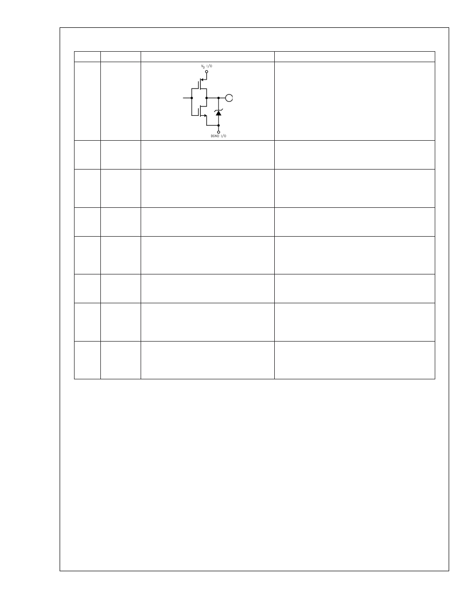
D0 - D11
Digital output word, CMOS compatible. D0 (pin 14) is
LSB, D11 (pin 27) is MSB. Load with no more than
50pF.
3
V
IN com
Analog input common. Connect to a quiet point in
analog ground near the driving device. See section
1.2.
5
V
A
Positive analog supply pin. Connect to a clean, quiet
voltage source of +5V. V
A
and V
D
should have a
common supply and be separately bypassed with a
5µF to 10µF capacitor and a 0.1µF chip capacitor.
4, 6
AGND
The ground return for the analog supply. AGND and
DGND should be connected together close to the
ADC12081 package. See section 5.0.
13
V
D
Positive analog supply pin. Connect to a clean, quiet
voltage source of +5V. V
A
and V
D
should have a
common supply and be separately bypassed with a
5µF to 10µF capacitor and a 0.1 µF chip capacitor.
9, 12
DGND
The ground return for the analog supply. AGND and
DGND should be connected together close to the
ADC12081 package. See section 5.0
21
V
D
I/O
The digital output driver supply pin. This pin can be
operated from a supply voltage of 3V to 5V, but the
voltage on this pin should never exceed the V
D
supply pin voltage.
20
DGND I/O
The ground return for the output drivers. This pin
should be returned to a point in the digital ground
that is removed from the other ground pins of the
ADC12081.
ADC12081
www.national.com
4