Pin descriptions and equivalent circuits #2 – Rainbow Electronics ADC12081 User Manual
Page 3
Pin Descriptions and Equivalent Circuits #2
No.
Symbol
Equivalent Circuit
Description
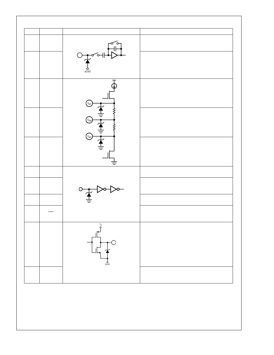
2
V
IN
Analog signal input. With a 2.0V reference voltage,
input signal voltages in the range of 0 to 2.0 Volts
will be converted. See section 1.2.
1
V
REF
Reference voltage input. This pin should be driven
from an accurate, stable reference source in the
range of 1.8 to 2.2V and bypassed to a low-noise
analog ground with a monolithic ceramic capacitor,
nominally 0.01µF. See section 1.1.
32
V
RP
Positive reference bypass pin. Bypass with a 0.1µF
capacitor. Do not connect anything else to this pin.
See section 3.1
31
V
RM
Reference midpoint bypass pin. Bypass with a 0.1µF
capacitor. Do not connect anything else to this pin.
See section 3.1
30
V
RN
Negative reverence bypass pin. Bypass with a 0.1µF
capacitor. Do not connect anything else to this pin.
See section 3.1
10
CLOCK
Sample Clock input, TTL compatible. Maximum
amplitude should not exceed 3V.
8
CAL
Calibration request, active High. Calibration cycle
starts when CAL returns to logic low. CAL is ignored
during power-down mode. See section 2.2.
7
PD
Power-down, active High, ignored during calibration
cycle. See paragraph 2.4
11
OE
Output enable control, active low. When this pin is
high the data outputs are in Tri-state
(high-impedance) mode.
28
OR
Over range indicator. This pin is at a logic High for
V
IN
<
0 or for V
IN
>
V
REF
.
29
READY
Device ready indicator, active High. This pin is at a
logic Low during a calibration cycle and while the
device is in the power down mode.
ADC12081
www.national.com
3