Operation – Rainbow Electronics DS1677 User Manual
Page 2
DS1677
2 of 17
Automatic backup and write protection of an external SRAM is provided through the V
CCO
and
CE0
pins.
The backup energy source used to power the RTC is also used to retain RAM data in the absence of V
CC
through the V
CCO
pin. The chip-enable output to SRAM,
CE0
, is controlled during power transients to
prevent data corruption.
The microprocessor monitor circuitry of the DS1677 provides three basic functions. First, a precision
temperature–compensated reference and comparator circuit monitors the status of V
CC
. When an out–of–
tolerance condition occurs, an internal power–fail signal is generated which forces the to
RST
the active
state. When V
CC
returns to an in–tolerance condition, the
RST
signal is kept in the active state for
250 ms to allow the power supply and processor to stabilize. The DS1677 debounces a push–button input
and guarantees an active
RST
pulse width of 250 ms. The third function is a watchdog timer. The
DS1677 has an internal timer that forces the
RST
signal to the active state if the strobe input is not driven
low prior to watchdog time–out.
The DS1677 also provides a 3–channel 8–bit successive approximation analog–to–digital converter. The
converter has an internal 2.55 volt (typical) reference voltage generated by an on–board band–gap circuit.
The A/D converter is monotonic (no missing codes) and has an internal analog filter to reduce high
frequency noise.
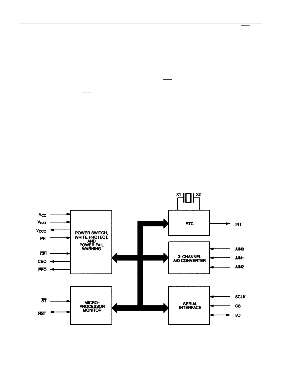
OPERATION
The block diagram in Figure 1 shows the main elements of the DS1677. The following paragraphs
describe the function of each pin.
DS1677 BLOCK DIAGRAM Figure 1