Clock accuracy (dip module), Clock accuracy (powercap module), Retrieving data from ram or clock – Rainbow Electronics DS1646P User Manual
Page 4
DS1646/DS1646P
4 of 11
CLOCK ACCURACY (DIP MODULE)
The DS1646 is guaranteed to keep time accuracy to within
±
1 minute per month at 25
°
C. The RTC is
calibrated at the factory by Dallas Semiconductor using nonvolatile tuning elements, and does not require
additional calibration. For this reason, methods of field clock calibration are not available and not
necessary. Clock accuracy is also effected by the electrical environment and caution should be taken to
place the RTC in the lowest level EMI section of the PCB layout. For additional information please see
application note 58.
CLOCK ACCURACY (POWERCAP MODULE)
The DS1646 and DS9034PCX are each individually tested for accuracy. Once mounted together, the
module will typically keep time accuracy to within
±
1.53 minutes per month (35 ppm) at 25°C. Clock
accuracy is also effected by the electrical environment and caution should be taken to place the RTC in
the lowest level EMI section of the PCB layout. For additional information please see application note
58.
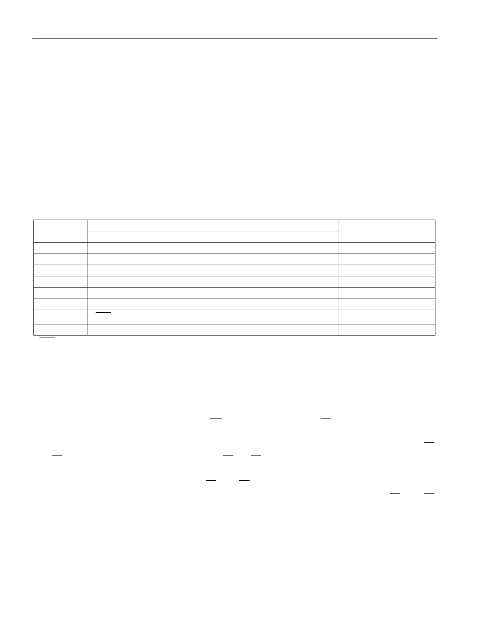
1646 REGISTER MAP - BANK1 Table 2
DATA
ADDRESS
B
7
B
6
B
5
B
4
B
3
B
2
B
1
B
0
FUNCTION
1FFFF
-
-
-
-
-
-
-
-
YEAR
00-99
1FFFE
X
X
X
-
-
-
-
-
MONTH
01-12
1FFFD
X
X
-
-
-
-
-
-
DATE
01-31
1FFFC
X
FT
X
X
X
-
-
-
DAY
01-07
1FFFB
X
X
-
-
-
-
-
-
HOUR
00-23
1FFFA
X
-
-
-
-
-
-
-
MINUTES
00-59
1FFF9
OSC
-
-
-
-
-
-
-
SECONDS
00-59
1FFF8
W
R
X
X
X
X
X
X
CONTROL
A
OSC
= STOP BIT
R = READ BIT
FT = FREQUENCY TEST
W = WRITE BIT
X = UNUSED
NOTE:
All indicated “X” bits are not dedicated to any particular function and can be used as normal RAM bits.
RETRIEVING DATA FROM RAM OR CLOCK
The DS1646 is in the read mode whenever
WE
(write enable) is high;
CE
(chip enable) is low. The
device architecture allows ripple-through access to any of the address locations in the NVSRAM. Valid
data will be available at the DQ pins within t
AA
after the last address input is stable, providing that the
CE
and
OE
access times and states are satisfied. If
CE
or
OE
access times are not met, valid data will be
available at the latter of chip-enable access (t
CEA
) or at output enable access time (t
OEA
). The state of the
data input/output pins (DQ) is controlled by
CE
and
OE
. If the outputs are activated before t
AA
, the data
lines are driven to an intermediate state until t
AA
. If the address inputs are changed while
CE
and
OE
remain valid, output data will remain valid for output data hold time (t
OH
) but will then go indeterminate
until the next address access.