Irlts6342pbf, Power mosfets – Rainbow Electronics IRLTS6342TRPBF User Manual
Page 5
IRLTS6342PbF
www.irf.com
5
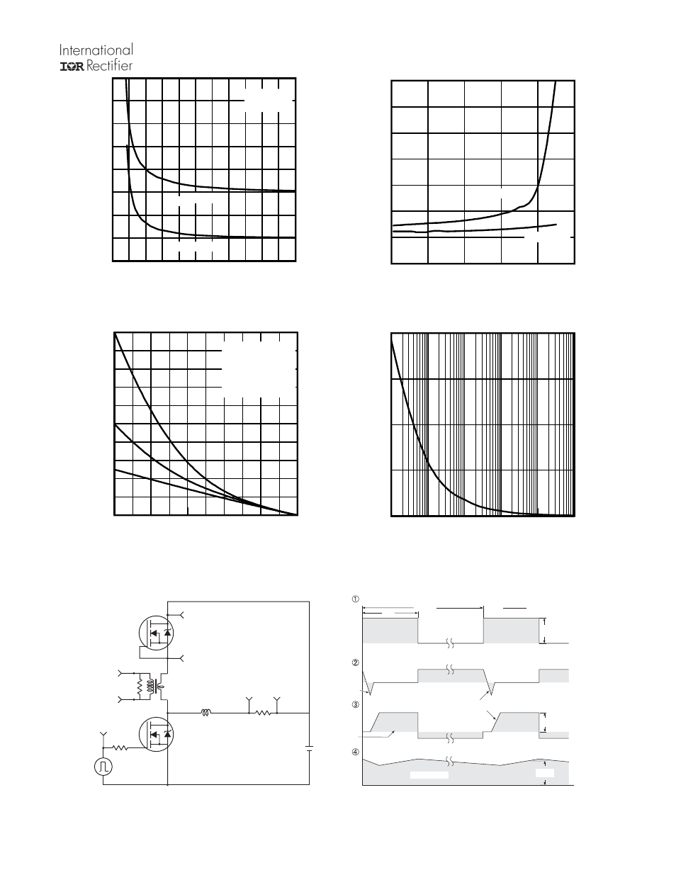
Fig 13. Typical On-Resistance vs. Drain Current
Fig 12. On-Resistance vs. Gate Voltage
Fig 15. Typical Power vs. Time
Fig 14. Maximum Avalanche Energy vs. Drain Current
Fig 16.
Peak Diode Recovery dv/dt Test Circuit for N-Channel
HEXFET
®
Power MOSFETs
Circuit Layout Considerations
• Low Stray Inductance
• Ground Plane
• Low Leakage Inductance
Current Transformer
P.W.
Period
di/dt
Diode Recovery
dv/dt
Ripple
≤ 5%
Body Diode Forward Drop
Re-Applied
Voltage
Reverse
Recovery
Current
Body Diode Forward
Current
V
GS
=10V
V
DD
I
SD
Driver Gate Drive
D.U.T. I
SD
Waveform
D.U.T. V
DS
Waveform
Inductor Curent
D =
P.W.
Period
*
V
GS
= 5V for Logic Level Devices
*
+
-
+
+
+
-
-
-
R
G
V
DD
• dv/dt controlled by R
G
• Driver same type as D.U.T.
• I
SD
controlled by Duty Factor "D"
• D.U.T. - Device Under Test
D.U.T
1E-8
1E-7
1E-6
1E-5
1E-4
1E-3
Time (sec)
0
4000
8000
12000
16000
P
ow
er
(
W
)
0
10
20
30
40
50
ID, Drain Current (A)
0
10
20
30
40
50
60
70
R
D
S
(o
n)
,
D
ra
in
-t
o
-S
ou
rc
e
O
n
R
es
is
ta
nc
e
(m
Ω
)
Vgs = 2.5V
Vgs = 4.5V
25
50
75
100
125
150
Starting TJ , Junction Temperature (°C)
0
10
20
30
40
50
60
70
80
90
100
E
A
S
,
S
in
gl
e
P
ul
se
A
va
la
nc
he
E
ne
rg
y
(m
J)
ID
TOP 0.9A
1.5A
BOTTOM 6.4A
1
2
3
4
5
6
7
8
9 10 11 12
VGS, Gate -to -Source Voltage (V)
5
10
15
20
25
30
35
40
45
R
D
S
(o
n)
,
D
ra
in
-t
o
-S
ou
rc
e
O
n
R
es
is
ta
nc
e
(m
Ω
)
ID = 8.0A
TJ = 25°C
TJ = 125°C