Converter electrical characteristics – Rainbow Electronics ADC08060 User Manual
Page 5
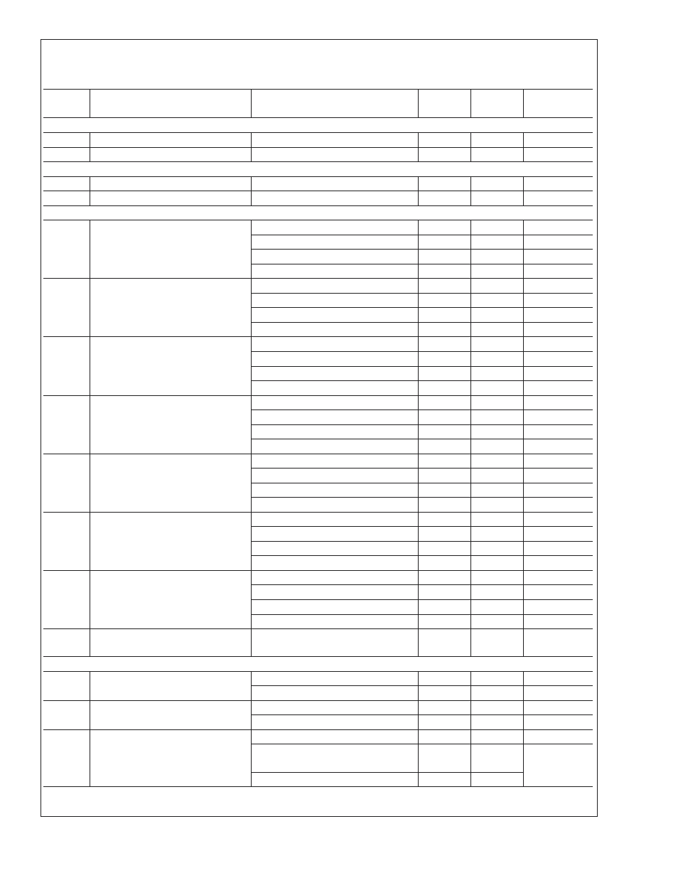
Converter Electrical Characteristics
(Continued)
The following specifications apply for V
A
= DR V
D
= +3.0V
DC
, V
RT
= +1.9V, V
RB
= 0.3V, C
L
= 10 pF, f
CLK
= 60 MHz at 50%
duty cycle. Boldface limits apply for T
J
= T
MIN
to T
MAX
: all other limits T
A
= 25˚C (Notes 7, 8)
Symbol
Parameter
Conditions
Typical
Limits
Units
(Limits)
CLK, PD DIGITAL INPUT CHARACTERISTICS
I
IL
Logical Low Input Current
V
IL
= 0V, DR V
D
= V
A
= 2.7V
−50
nA
C
IN
Logic Input Capacitance
3
pF
DIGITAL OUTPUT CHARACTERISTICS
V
OH
High Level Output Voltage
V
A
= DR V
D
= 2.7V, I
OH
= −400 µA
2.6
2.4
V (min)
V
OL
Low Level Output Voltage
V
A
= DR V
D
= 2.7V, I
OL
= 1.0 mA
0.4
0.5
V (max)
DYNAMIC PERFORMANCE
ENOB
Effective Number of Bits
f
IN
= 4.4 MHz, V
IN
= FS − 0.25 dB
7.6
Bits
f
IN
= 10 MHz, V
IN
= FS − 0.25 dB
7.6
7.1
Bits (min)
f
IN
= 25 MHz, V
IN
= FS − 0.25 dB
7.5
Bits
f
IN
= 29 MHz, V
IN
= FS − 0.25 dB
7.4
Bits
SINAD
Signal-to-Noise & Distortion
f
IN
= 4.4 MHz, V
IN
= FS − 0.25 dB
47
dB
f
IN
= 10 MHz, V
IN
= FS − 0.25 dB
47
44.5
dB (min)
f
IN
= 25 MHz, V
IN
= FS − 0.25 dB
47
dB
f
IN
= 29 MHz, V
IN
= FS − 0.25 dB
46
dB
SNR
Signal-to-Noise Ratio
f
IN
= 4.4 MHz, V
IN
= FS − 0.25 dB
47
dB
f
IN
= 10 MHz, V
IN
= FS − 0.25 dB
47
44.6
dB (min)
f
IN
= 25 MHz, V
IN
= FS − 0.25 dB
47
dB
f
IN
= 29 MHz, V
IN
= FS − 0.25 dB
46
dB
SFDR
Spurious Free Dynamic Range
f
IN
= 4.4 MHz, V
IN
= FS − 0.25 dB
64
dBc
f
IN
= 10 MHz, V
IN
= FS − 0.25 dB
63
dBc
f
IN
= 25 MHz, V
IN
= FS − 0.25 dB
60
dBc
f
IN
= 29 MHz, V
IN
= FS − 0.25 dB
54
dBc
THD
Total Harmonic Distortion
f
IN
= 4.4 MHz, V
IN
= FS − 0.25 dB
−64
dBc
f
IN
= 10 MHz, V
IN
= FS − 0.25 dB
−63
dBc
f
IN
= 25 MHz, V
IN
= FS − 0.25 dB
-57
dBc
f
IN
= 29 MHz, V
IN
= FS − 0.25 dB
−54
dBc
HD2
2nd Harmonic Distortion
f
IN
= 4.4 MHz, V
IN
= FS − 0.25 dB
-70
dBc
f
IN
= 10 MHz, V
IN
= FS − 0.25 dB
−65
dBc
f
IN
= 25 MHz, V
IN
= FS − 0.25 dB
-64
dBc
f
IN
= 29 MHz, V
IN
= FS − 0.25 dB
−54
dBc
HD3
3rd Harmonic Distortion
f
IN
= 4.4 MHz, V
IN
= FS − 0.25 dB
−72
dBc
f
IN
= 10 MHz, V
IN
= FS − 0.25 dB
−70
dBc
f
IN
= 25 MHz, V
IN
= FS − 0.25 dB
-68
dBc
f
IN
= 29 MHz, V
IN
= FS − 0.25 dB
−65
dBc
IMD
Intermodulation Distortion
f
1
= 11 MHz, V
IN
= FS − 6.25 dB
f
2
= 12 MHz, V
IN
= FS − 6.25 dB
-55
dBc
POWER SUPPLY CHARACTERISTICS
I
A
Analog Supply Current
DC Input
25
31
mA (max)
f
IN
= 10 MHz, V
IN
= FS − 3 dB
25
mA
DR I
D
Output Driver Supply Current
DC Input
0.3
1
mA (max)
f
IN
= 10 MHz, V
IN
= FS − 3 dB
4.4
mA
I
A
+
DRI
D
Total Operating Current
DC Input
25.3
32
mA (max)
f
IN
= 10 MHz, V
IN
= FS − 3 dB,
PD = Low
29.4
mA (max)
CLK Low, PD = Hi
0.2
ADC08060
www.national.com
5