Rainbow Electronics DS1780 User Manual
Page 27

DS1780
27 of 28
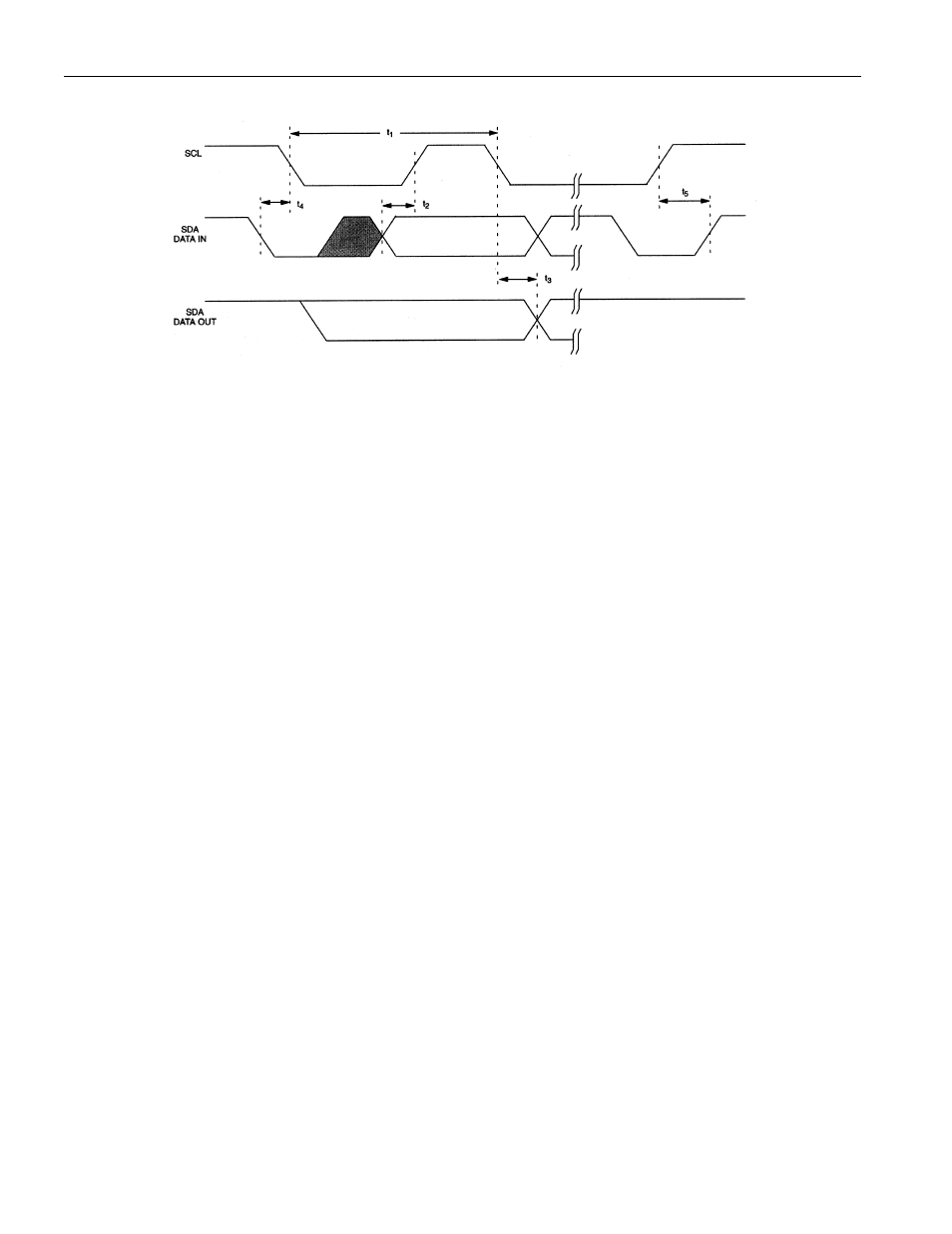
2-WIRE BUS TIMING DIAGRAM Figure 8
NOTES:
1. All voltages are referenced to ground, unless otherwise specified.
2. When the input voltage (VIN) at any pin exceeds the power supplies (V
IN
< (GND or GNDA) or V
IN
>V
DD
, except for analog voltage inputs), the current at that pin should be limited to 5 mA. The 20 mA
maximum package input current rating limits the number of pins that can safely exceed the power
supplies with an input current of 5 mA to four.
3. Solder according to IPC standards.
4. IDD specified with open-drain output pin open.
5. IDD specified with V
CC
at 5.0V and SDA, SCL = 5.0V.
6. TUE (Total Unadjusted Error) includes Offset, Gain and Linearity errors of the ADC.
7. Monitoring Cycle Time includes temperature conversion, voltage conversions, and fan speed
readings.
8. The total fan count is based on 2 pulses per revolution of the fan tachometer output.
9. Limits (Min and Max specs) are defined for the full temperature range -40°C
≤
T
A
≤
+125°C and
voltage range 2.8V
≤
V
DD
≤
5.75V, unless otherwise stated as a condition. Typical values represent
parametric norms at T
A
= 25°C at 4.5V
≤
V
DD
≤
5.5V, unless otherwise stated as a condition.
