Retrieving data from ram or clock, Writing data to ram or clock, Data retention mode – Rainbow Electronics DS1643P User Manual
Page 4
DS1643/DS1643P
4 of 14
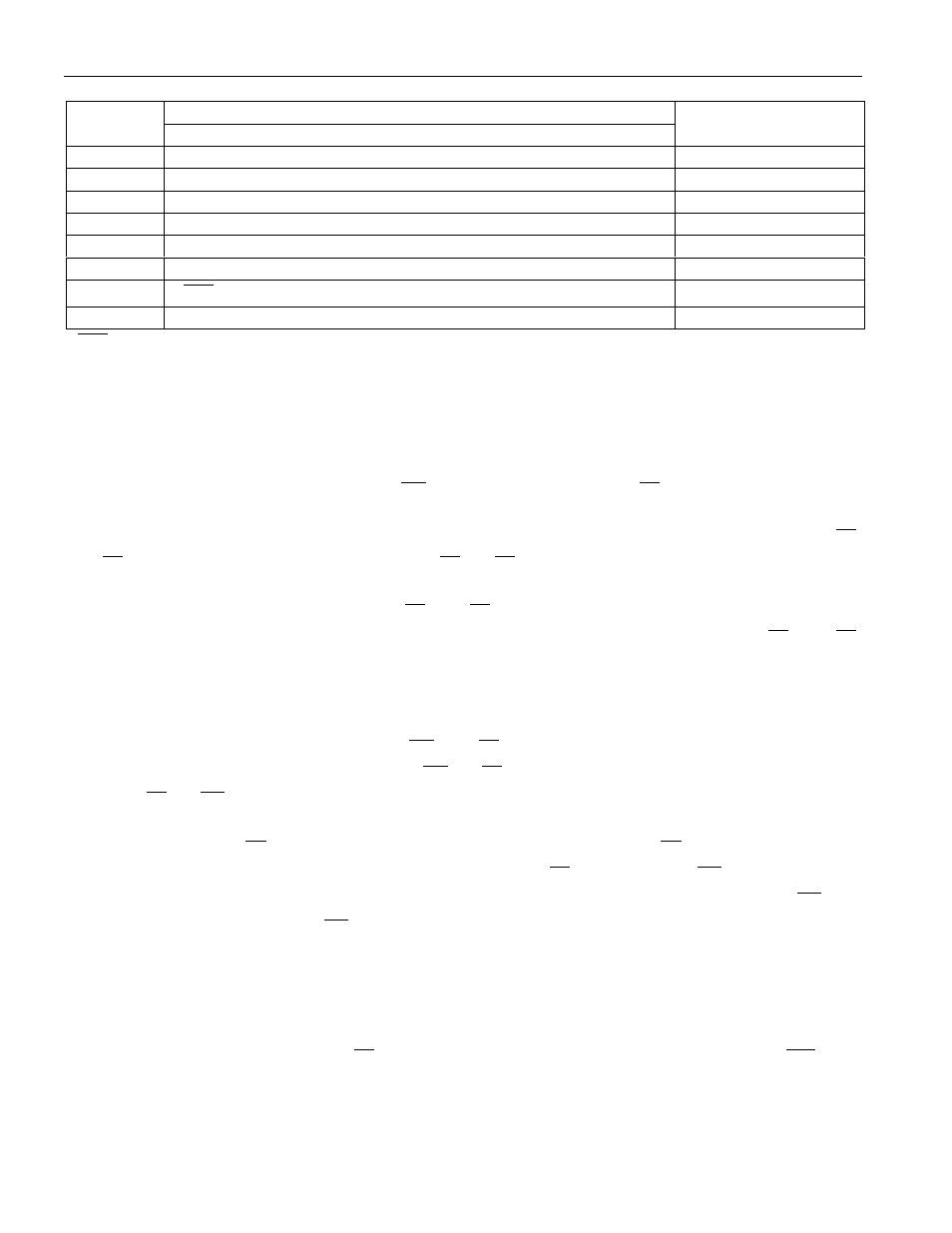
DS1643 REGISTER MAP - BANK1 Table 2
DATA
ADDRES
S
B
7
B
6
B
5
B
4
B
3
B
2
B
1
B
0
FUNCTION
1FFF
-
-
-
-
-
-
-
-
YEAR
00-99
1FFE
X
X
X
-
-
-
-
-
MONTH
01-12
1FFD
X
X
-
-
-
-
-
-
DATE
01-31
1FFC
X
FT
X
X
X
-
-
-
DAY
01-07
1FFB
X
X
-
-
-
-
-
-
HOUR
00-23
1FFA
X
-
-
-
-
-
-
-
MINUTES
00-59
1FF9
OSC
-
-
-
-
-
-
-
SECONDS
00-59
1FF8
W
R
X
X
X
X
X
X
CONTROL
A
OSC
= STOP BIT
R = READ BIT
FT = FREQUENCY TEST
W = WRITE BIT
X = UNUSED
NOTE:
All indicated “X” bits are not dedicated to any particular function and can be used as normal RAM bits.
RETRIEVING DATA FROM RAM OR CLOCK
The DS1643 is in the read mode whenever
WE
(write enable) is high and
CE
(chip enable) is low. The
device architecture allows ripple-through access to any of the address locations in the NV SRAM. Valid
data will be available at the DQ pins within t
AA
after the last address input is stable, providing that the
CE
and
OE
access times and states are satisfied. If
CE
or
OE
access times are not met, valid data will be
available at the latter of chip enable access (t
CEA
) or at output enable access time (t
OEA
). The state of the
data input/output pins (DQ) is controlled by
CE
and
OE
. If the outputs are activated before t
AA
, the data
lines are driven to an intermediate state until t
AA
. If the address inputs are changed while
CE
and
OE
remain valid, output data will remain valid for output data hold time (t
OH
) but will then go indeterminate
until the next address access.
WRITING DATA TO RAM OR CLOCK
The DS1643 is in the write mode whenever
WE
and
CE
are in their active state. The start of a write is
referenced to the latter occurring transition of
WE
or
CE
. The addresses must be held valid throughout
the cycle.
CE
or
WE
must return inactive for a minimum of t
WR
prior to the initiation of another read or
write cycle. Data in must be valid t
DS
prior to the end of write and remain valid for t
DH
afterward. In a
typical application, the
OE
signal will be high during a write cycle. However,
OE
can be active provided
that care is taken with the data bus to avoid bus contention. If
OE
is low prior to
WE
transitioning low
the data bus can become active with read data defined by the address inputs. A low transition on
WE
will
then disable the outputs t
WEZ
after
WE
goes active.
DATA RETENTION MODE
When V
CC
is within nominal limits (V
CC
> 4.5 volts) the DS1643 can be accessed as described above with
read or write cycles. However, when V
CC
is below the power-fail point V
PF
(point at which write
protection occurs) the internal clock registers and RAM are blocked from access. This is accomplished
internally by inhibiting access via the
CE
signal. At this time the power-on reset output signal (
RST
) will
be driven active low and will remain active until V
CC
returns to nominal levels. When V
CC
falls below the
level of the internal battery supply, power input is switched from the V
CC
pin to the internal battery and
clock activity, RAM, and clock data are maintained from the battery until V
CC
is returned to nominal