Detailed pin description – Rainbow Electronics DS2715 User Manual
Page 4
DS2715: NiMH Cell Pack Charge Controller
4 of 12
Note 1:
Voltages relative to V
SS
.
Note 2:
Does not include current through V
CH
, R
T
, and DIV pins.
Note 3:
Below this voltage no I/O pins are active.
Note 4:
Does not include tolerance of R
T
resistor.
Note 5:
V
BIAS
and resistor tolerances must be added to determine actual threshold.
Note 6:
Specified temperature thresholds are only valid if recommended thermistor types are used.
Note 7:
Specification is guaranteed by design.
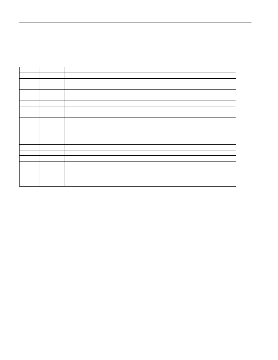
DETAILED PIN DESCRIPTION
PIN
NAME
DESCRIPTION
1 C
BIAS
Bypass for Internal Voltage Regulator
2 V
CH
Cell Stack Charge Control Output
3 V
SS
Ground Reference and Chip Supply Return
4 LED1
Charging
Indicator
Output
5 LED2
Done
Indicator
Output
6 V
SS
Ground Reference and Chip Supply Return
7
CTG
Connect to Ground
8
CTG
Connect to Ground
9 MODE
Mode Select. Connect to V
SS
for linear mode of operation or C
BIAS
for comparator
mode of operation.
10 DIV
Thermistor Divider. Stable output to form a resistor divider for measuring
temperature on THM.
11
SNS+
Positive Current Sense. Connect to the pack side of the sense resistor.
12
SNS-
Negative Current Sense. Connect to the cell stack side of the sense resistor.
13 V
DD
Chip Supply Input: +4.0V to +5.5V range.
14 R
T
Failsafe Timeout. Timeout is selected by an external resistor from R
T
to V
SS
.
15 THM
Thermistor Input. Connect to a thermistor located in the cell pack and a divider
resistor from the Div pin.
16 V
BATT
Battery Voltage Sense Input. Connect to a divider from the positive terminal of the
cell stack to measure the voltage of a single cell.