Absolute maximum ratings, Recommended dc operating conditions, Dc electrical characteristics – Rainbow Electronics DS2715 User Manual
Page 2
DS2715: NiMH Cell Pack Charge Controller
2 of 12
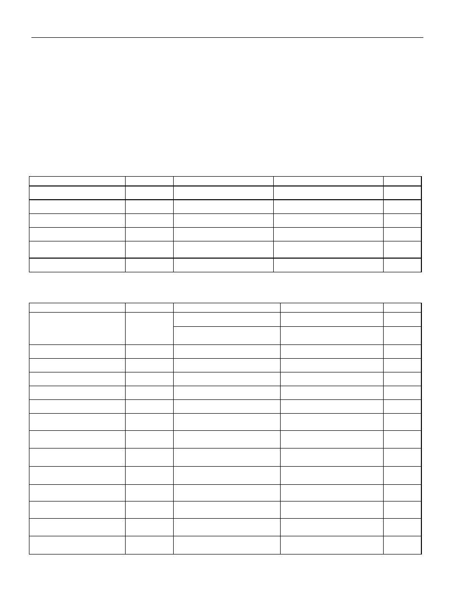
ABSOLUTE MAXIMUM RATINGS*
Voltage on V
DD
and V
CH
Pins with Respect to V
SS
-0.3V to +18V
Voltage on LED1 and LED2 Pins
-0.3V to +18V
Voltage on SNS-
-0.3V to +0.3V
Voltage on C
BIAS
-0.3V
to
6V
Voltage on all Other Pins
-0.3V to V
Cbias
Continuous Sink Current V
CH
, LED1, and LED2
28mA
Operating Temperature Range
-20°C to +85°C
Storage Temperature Range
-55°C to +125°C
Soldering
Temperature
See
IPC/JEDECJ-STD-020
*This is a stress rating only and functional operation of the device at these or any other conditions above those indicated in the operation
sections of this specification is not implied. Exposure to absolute maximum rating conditions for extended periods of time may affect reliability.
RECOMMENDED DC OPERATING CONDITIONS
(4.5V
£ V
DD
£ 16.5V; T
A
= 0
°C to +70°C.)
PARAMETER SYMBOL CONDITIONS MIN
TYP
MAX
UNITS
Supply Voltage
V
DD
(Note
1)
4.5 16.5 V
LED1, LED2 Voltage
V
LED
(Note
1)
0.0
16.5
V
Mode Voltage
V
MODE
(Note
1)
0.0
V
Cbias
V
V
CH
Voltage
V
VCH
(Note
1)
0.0
16.5
V
C
BIAS
Capacitor Range
C
Cbias
.02
.15
µF
R
T
Resistor Range
R
Rt
20
240 KΩ
DC ELECTRICAL CHARACTERISTICS
(4.5V
£ V
DD
£ 16.5V, T
A
= 0
°C to +70°C, unless otherwise noted.)
PARAMETER SYMBOL CONDITIONS MIN
TYP
MAX
UNITS
Linear Mode, V
DD
= 16.5V
1.3
1.6
mA
Operating Current
(Note 2)
I
DDA
Comparator Mode,
V
DD
= 16.5V
150 250 µA
Idle Current
I
DDS
V
DD
< V
UVLO
10
µA
Discharge Current
I
DDD
Discharge latch set (Note 2)
200
µA
UVLO Threshold
V
UVLO
V
DD
Rising (Note 3)
3.8
3.9
4.0
V
UVLO Hysteresis
V
UVLO-HYS
V
DD
Falling
35
mV
V
CH
Sink Current
I
OL-Vch
V
OL
= 1.5V
20
mA
LED1, LED2 Sink Current
I
OL-LED
V
OL
= 1.0V
20
mA
Leakage Current, V
CH
,
LED1, LED2
I
LKG
Pin inactive or Device Idle
-1
+1
µA
THM Pin Leakage
Current
I
LKG-THM
-1
+1
µA
V
BATT
Pin Leakage
Current
I
LKG-Vbatt
-50
+50
nA
C
BIAS
Voltage
V
Cbias
0 < I
Cbias
< 0.4ma
3.9
4.0
4.3
V
DIV Pin Load Current
I
Div
500 uA
Current Sense Amplifier
Gain
G
ERR
100µA < I
Vch
< 20mA
5
6.25
7.5
Ω
-1
Current Sense
Comparator Gain
G
COMP
(Note
7)
10
Ω
-1