Converter electrical characteristics, Adc1 173 – Rainbow Electronics ADC1173 User Manual
Page 6
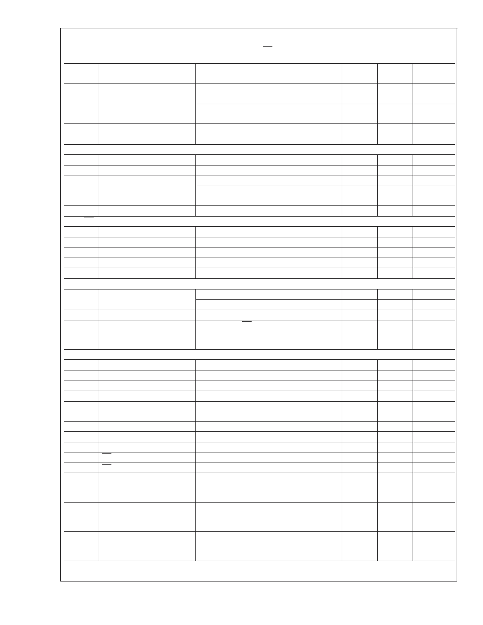
Converter Electrical Characteristics
(Continued)
The following specifications apply for AV
DD
= DV
DD
= +3.0V
DC
, OE = 0V, V
RT
= +2.0V, V
RB
= 0V, C
L
= 20 pF, f
CLK
= 15MHz
at 50% duty cycle. Boldface limits apply for T
A
= T
MIN
to T
MAX
; all other limits T
A
= 25˚C (Notes 7, 8)
Symbol
Parameter
Conditions
Typical
Limits
Units
V
RTS
-
V
RBS
Self Bias Voltage Delta
V
RT
connected to V
RTS
,
V
RB
connected to V
RBS
1.2
1.1
1.3
µAmin
µAmax
V
RT
connected to V
RTS
,
V
RB
connected to V
SS
1.38
V
V
RT
- V
RB
Reference Voltage Delta
2
1.0
V(min)
V
A
V(max)
Power Supply Characteristics
IA
DD
Analog Supply Current
DV
DD
= AV
DD
= 3.6V
6.8
mA
ID
DD
Digital Supply Current
DV
DD
= AV
DD
= 3.6V
2.3
mA
IAV
DD
+
IDV
DD
Total Operating Current
DV
DD
AV
DD
= 3.6V,
9.1
11.4
mA
DV
DD
= AV
DD
= 3.6V, CLK Low
5.8
mA
Power Consumption
DV
DD
= AV
DD
= 3.6V
33
41
mW
CLK, OE Digital Input Characteristics
V
IH
Logical High Input Voltage
DV
DD
= AV
DD
= 3.6V
2.2
V (min)
V
IL
Logical Low Input Voltage
DV
DD
= AV
DD
= 3.6V
0.8
V (max)
I
IH
Logical High Input Current
V
IH
= DV
DD
= AV
DD
= 3.6V
5
µA
I
IL
Logic Low Input Current
V
IL
= 0V, DV
DD
= AV
DD
= 3.6V
−5
µA
C
IN
Logic Input Capacitance
5
pF
Digital Output Characteristics
V
OH
High Level Output Voltage
DV
DD
= 2.7V, I
OH
= −360µA
2.4
V(min)
DV
DD
= 2.7V, I
OH
= −1.1mA
2.1
1.9
V(min)
V
OL
Low Level Output Voltage
DV
DD
= 2.7V, I
OL
= 1.6mA
0.32
0.6
V(max)
I
OZH
,
I
OZL
TRI-STATE
®
Leakage Current
DV
DD
= 3.6V, OE = DV
DD
,
V
OL
= 0V or V
OH
= DV
DD
±
20
µA
AC Electrical Characteristics
f
C1
Maximum Conversion Rate
20
15
MHz(min)
f
C2
Minimum Conversion Rate
1
MHz
t
OD
−0
Output Delay
CLK high to low data valid
28
ns(max)
t
OD
−1
Output Delay
CLK low to high data valid
24
ns(max)
Pipeline Delay (Latency)
2.5
Clock
Cycles
t
DS
Sampling (Aperture) Delay
CLK low to acquisition of data
3
ns
t
AJ
Aperture Jitter
30
ps rms
t
OH
Output Hold Time
CLK high to data invalid
15
ns
t
EN
OE Low to Data Valid
Loaded as in Figure 2
22
ns
t
DIS
OE High to High Z State
Loaded as in Figure 2
12
ns
ENOB
Effective Number of Bits
f
IN
= 1.31 MHz
f
IN
= 3.58 MHz
f
IN
= 7.5 MHz
7.7
7.6
7.4
7.0
Bits (min)
SINAD
Signal-to- Noise & Distortion
f
IN
= 1.31 MHz
f
IN
= 3.58 MHz
f
IN
= 7.5 MHz
49
47.7
46.5
43
dB(min)
SNR
Signal-to-Noise Ratio
f
IN
= 1.31 MHz
f
IN
= 3.58 MHz
f
IN
= 7.5 MHz
49
48.7
48.0
44
dB(min)
ADC1
173
www.national.com
6