Rainbow Electronics ADC1173 User Manual
General description, Features, Key specifications
ADC1173
8-Bit, 3-Volt, 15MSPS, 33mW A/D Converter
General Description
The ADC1173 is a low power, 15 MSPS analog-to-digital
converter that digitizes signals to 8 bits while consuming just
33 mW of power (typ). The ADC1173 uses a unique archi-
tecture that achieves 7.6 Effective Bits. Output formatting is
straight binary coding.
The excellent DC and AC characteristics of this device,
together with its low power consumption and +3V single
supply operation, make it ideally suited for many video,
imaging and communications applications, including use in
portable equipment. Furthermore, the ADC1173 is resistant
to latch-up and the outputs are short-circuit proof. The top
and bottom of the ADC1173’s reference ladder is available
for connections, enabling a wide range of input possibilities.
The ADC1173 is offered in SOIC (EIAJ) and TSSOP. It is
designed to operate over the commercial temperature range
of -40˚C to +75˚C.
Features
n
Internal Sample-and-Hold Function
n
Single +3V Operation
n
Internal Reference Bias Resistors
n
Industry Standard Pinout
n
TRI-STATE
®
Outputs
Key Specifications
n
Resolution
8 Bits
n
Maximum Sampling Frequency
15 MSPS (min)
n
THD
−54 dB (typ)
n
DNL
±
0.85 LSB (max)
n
ENOB at 3.58 MHz Input
7.6 Bits (typ)
n
Guaranteed No Missing Codes
n
Differential Phase
0.5 Degree (max)
n
Differential Gain
1.5% (typ)
n
Power Consumption
33mW (typ)
n
(excluding reference current)
Applications
n
Video Digitization
n
Digital Still Cameras
n
Set Top Boxes
n
Camcorders
n
Personal Computer Video
n
Digital Television
n
CCD Imaging
n
Electro-Optics
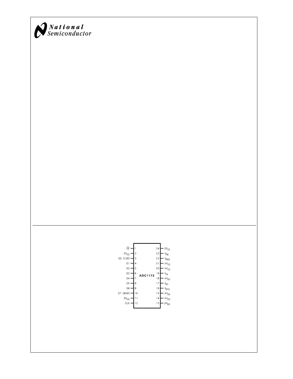
Pin Configuration
10089001
TRISTATE&
®
is a registered trademark of National Semiconductor Corporation.
March 2003
ADC1
173
8-Bit,
3-V
olt,
15MSPS,
33mW
A/D
Converter
© 2003 National Semiconductor Corporation
DS100890
www.national.com
Document Outline
- ADC1173
- General Description
- Features
- Key Specifications
- Applications
- Pin Configuration
- Ordering Information
- Block Diagram
- Pin Descriptions and Equivalent Circuits
- Absolute Maximum Ratings
- Operating Ratings(Notes , )
- Converter Electrical Characteristics
- Typical Performance Characteristics
- Specification Definitions
- Timing Diagram
- FIGURE 2. tEN, tDISTest Circuit
- Functional Description
- Applications Information
- 1.0 THE ANALOG INPUT
- 2.0 REFERENCE INPUTS
- FIGURE 3. Simple, Low Component Count, Self -Bias Reference application. Because of resistor toleran
- FIGURE 4. Better defining the ADC Reference Voltage. Self-bias is still used, but the reference volt
- FIGURE 5. Driving the reference to force desired values requires driving with a low impedance source
- 3.0 POWER SUPPLY CONSIDERATIONS
- 4.0 THE ADC1173 CLOCK
- 5.0 LAYOUT AND GROUNDING
- FIGURE 6. Layout example showing separate analog and digital ground planes connected below the ADC11
- 6.0 DYNAMIC PERFORMANCE
- FIGURE 7. Isolating the ADC clock from Digital Circuitry.
- 7.0 COMMON APPLICATION PITFALLS
- FIGURE 8. 5.5 MHz Low Pass Filter to Eliminate Harmonics at the Signal Input.
- FIGURE 9. 11 MHz Low Pass filter to eliminate harmonics at the signal input. Use at input frequencie
- Physical Dimensions