Absolute maximum ratings, Operating ratings(notes , ), Converter electrical characteristics – Rainbow Electronics ADC1173 User Manual
Page 5: Operating ratings, Adc1 173
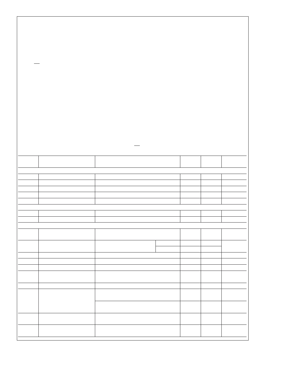
Absolute Maximum Ratings
If Military/Aerospace specified devices are required,
please contact the National Semiconductor Sales Office/
Distributors for availability and specifications.
AV
DD
, DV
DD
6.5V
Voltage on Any Pin
−0.3V to 6.5V
V
RT
, V
RB
AV
DD
to V
SS
CLK, OE Voltage
−0.5 to (AV
DD
+ 0.5V)
Digital Output Voltage
DV
SS
to DV
DD
Input Current (Note 3)
±
25mA
Package Input Current
±
50mA
Package Dissipation at 25˚C
ESD Susceptibility (Note 5)
Human Body Model
2000V
Machine Model
200V
Soldering Temp., Infrared, 10
sec. (Note 6)
300˚C
Storage Temperature
−65˚C to +150˚C
Operating Ratings
(Notes 1, 2)
Temperature Range
−40˚C
≤ T
A
≤ +75˚C
AV
DD
, DV
DD
+2.7V to +3.6V
|AV
SS
-DV
SS
|
0V to 100 mV
V
RT
1.0V to AV
DD
V
RB
0V to 2.0V
RT
-
RB
1.0V to 2.8V
V
IN
Voltage Range
V
RB
to V
RT
Converter Electrical Characteristics
The following specifications apply for AV
DD
= DV
DD
= +3.0V
DC
, OE = 0V, V
RT
= +2.0V, V
RB
= 0V, C
L
= 20 pF, f
CLK
= 15MHz
at 50% duty cycle. Boldface limits apply for T
A
= T
MIN
to T
MAX
; all other limits T
A
= 25˚C (Notes 7, 8)
Symbol
Parameter
Conditions
Typical
Limits
Units
DC Accuracy
INL
Integral Non Linearity
±
0.5
±
1.3
LSB( max)
DNL
Differential Non Linearity
±
0.4
±
0.85
LSB( max)
Missing Codes
0
(max)
E
OT
Top Offset
−12
mV
E
OB
Bottom Offset
+1.0
mV
Video Accuracy
DP
Differential Phase Error
f
in
= 3.58 MHz sine wave
0.5
Degree
DG
Differential Gain Error
f
in
= 3.58 MHz sine wave
1.5
%
Analog Input and Reference Characteristics
V
IN
Input Range
2.0
V
RB
V
RT
V(min)
V(max)
C
IN
V
IN
Input Capacitance
V
IN
= 1.5V + 0.7Vrms
(CLK LOW)
4
pF
(CLK HIGH)
11
R
IN
Input Resistance
>
1
M
Ω
BW
Analog Input Bandwidth
120
MHz
R
RT
Top Reference Resistor
360
Ω
R
REF
Reference Ladder Resistance
V
RT
to V
RB
300
200
Ω(min)
400
Ω(max)
R
RB
Bottom Reference Resistor
90
Ω
I
REF
Reference Ladder Current
V
RT
=V
RTS
, V
RB
=V
RBS
4.2
mA
V
RT
=V
RTS
,V
RB
=AV
SS
4.8
mA
V
RT
Reference Top Self Bias
Voltage
V
RT
connected to V
RTS
V
RB
connected to V
RBS
1.56
1.45
1.65
V(min)
V(max)
V
RB
Reference Bottom Self Bias
Voltage
V
RT
connected to V
RTS
0.36
0.32
V(min)
V
RB
connected to V
RBS
0.40
V(max)
ADC1
173
www.national.com
5