Absolute maximum ratings, Recommended operating conditions, Package thermal resistance (note 7) – Rainbow Electronics CLC5957 User Manual
Page 3: Reliability information, Converter electrical characteristics, Package thermal resistance, Clc5957
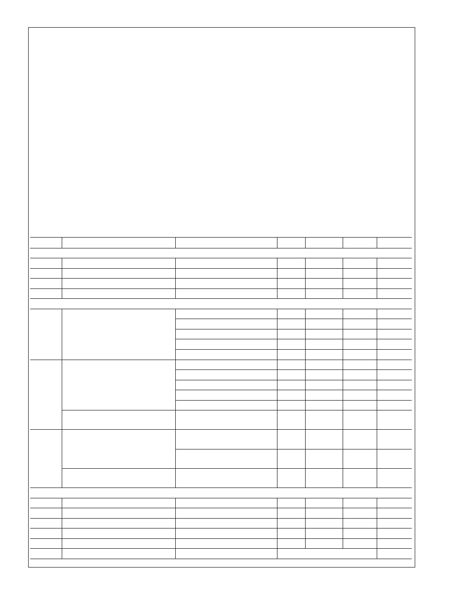
Absolute Maximum Ratings
If Military/Aerospace specified devices are required,
please contact the National Semiconductor Sales Office/
Distributors for availability and specifications.
Positive Supply Voltage (V
CC
)
−0.5V to +6V
Differential Voltage between any two
Grounds
<
100 mV
Analog Input Voltage Range
GND to V
CC
Digital Input Voltage Range
−0.5V to +V
CC
Output Short Circuit Duration
(one-pin to ground)
Infinite
Junction Temperature (Note 7)
175˚C
Storage Temperature Range
−65˚C to +150˚C
Lead Solder Duration (+300˚C)
10 sec.
ESD tolerance
human body model
machine model
2000V
200V
Recommended Operating
Conditions
Positive Supply Voltage (V
CC
)
+5V
±
5%
Analog Input Voltage Range
2.048 V
PP
diff.
Operating Temperature Range
−40˚C to +85˚C
Package Thermal Resistance
Package
θ
JA
θ
JC
48-Pin TSSOP
56˚C/W
16˚C/W
Reliability Information
Transistor Count
5000
Converter Electrical Characteristics
The following specifications apply for AV
CC
= DV
CC
= +5V, 66MSPS. Boldface limits apply for T
A
= T
min
= −40˚C to T
max
=
+85˚C, all other limits T
A
= 25˚C (Note 3).
Symbol
Parameter
Conditions
Min
Typ
Max
Units
DYNAMIC PERFORMANCE
BW
Large-Signal Bandwidth
A
IN
= −3 dBFS
300
MHz
Overvoltage Recovery Time
A
IN
= 1.5 FS (0.01%)
12
ns
t
A
Effective Aperture Delay
−0.41
ns
t
AJ
Aperture Jitter
0.3
ps(rms)
NOISE AND DISTORTION
SNR
*
Signal-to-Noise Ratio (without 50
harmonics)
f
IN
= 5 MHz, A
IN
= −1dBFS
67
dBFS
f
IN
= 25 MHz, A
IN
= −1dBFS
*
60
66
dBFS
f
IN
= 75 MHz, A
IN
= −3dBFS
65
dBFS
f
IN
= 150 MHz, A
IN
= −15dBFS
66
dBFS
f
IN
= 250 MHz, A
IN
= −15dBFS
66
dBFS
SFDR
Spurious-Free Dynamic Range
f
IN
= 5 MHz, A
IN
= −1dBFS
74
dBc
f
IN
= 25 MHz, A
IN
= −1dBFS
*
60
74
dBc
f
IN
= 75 MHz, A
IN
= −3dBFS
72
dBc
f
IN
= 150 MHz, A
IN
= −15dBFS
69
dBc
f
IN
= 250 MHz, A
IN
= −15dBFS
65
dBc
Spurious-Free Dynamic Range
(dithered)
f
IN
= 19 MHz, A
IN
= −6dBFS
85
dBFS
IMD
Intermodulation Distortion
f
IN1
= 149.84 MHz, f
IN2
= 149.7
MHz, A
IN
= −10dBFS
68
dBFS
f
IN1
= 249.86 MHz, f
IN2
= 249.69
MHz, A
IN
= −10dBFS
58
dBFS
Intermodulation Distortion (dithered)
f
IN1
= 74 MHz, f
IN2
= 75 MHz,
A
IN
= −12dBFS
83
dBFS
DC ACCURACY AND PERFORMANCE
DNL
Differential Non-Linearity
f
IN
= 5MHz, A
IN
= −1dBFS
±
0.65
LSB
INL
Integral Non-Linearity
f
IN
= 5MHz, A
IN
= −1dBFS
±
1.5
LSB
Offset Error (Note 2)
−30
0
30
mV
Gain Error
1.2
% FS
V
REF
Reference Voltage (Note 2)
2.2
2.37
2.6
V
No Missing Codes (Note 2)
f
IN
= 5MHz, A
IN
= -1dBFS
Guaranteed
CLC5957
www.national.com
3