Pin configuration, Ordering information, Pin descriptions – Rainbow Electronics CLC5957 User Manual
Page 2
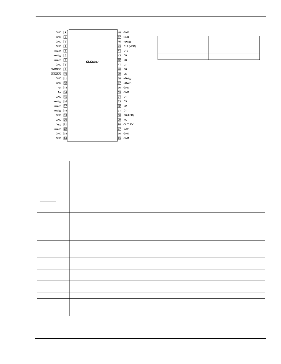
Pin Configuration
01502901
Ordering Information
CLC5957MTD
48-Pin TSSOP
CLC5957MTDX
48-Pin TSSOP (Taped
Reel)
CLC5957PCASM
Evaluation Board
Pin Descriptions
Pin
Name
Pin
No.
Description
A
IN
A
IN
13, 14
Differential input with a common mode voltage of +2.4V. The ADC
full scale input is 1.024 V
PP
on each of the complimentary input
signals.
ENCODE
ENCODE
9, 10
Differential clock where ENCODE initiates a new data conversion
cycle on each rising edge. Logic for these inputs are a 50% duty
cycle universal differential signal (
>
200mV). The clock input is
internally biased to V
CC
/2 with a termination impedance of 2.5k
Ω
.
V
CM
21
Internal common mode voltage reference. Nominally +2.4V. Can be
used for the input common mode voltage. This voltage is derived
from an internal bandgap reference. V
CM
should be buffered when
driving any external load. Failure to buffer this signal can cause
errors in the internal bias currents.
D0–D11
30–34,
39–45
Digital data outputs are CMOS and TTL compatible. D0 is the LSB
and D11 is the MSB. MSB is inverted. Output coding is two’s
complement. Current limited to source/sink 2.5mA typical.
GND
1–4, 8, 11, 12, 15, 19,
20, 23–26, 35, 36, 47, 48
Circuit ground.
+AV
CC
5–7, 16–18, 22
+5V power supply for the analog section. Bypass to ground with a
0.1 µF capacitor.
+DV
CC
37, 38, 46
+5V power supply for the digital section. Bypass to ground with a
0.1 µF capacitor.
NC
29
No connect. May be left open or grounded.
DAV
27
Data Valid Clock. Data is valid on rising edge. Current limited to
source/sink 5mA typical.
OUTLEV
28
Output Logic 3.3V or 2.5V option. Open = 3.3V, GND = 2.5V.
CLC5957
www.national.com
2