Clc5957 applications, Analog inputs and bias, Figure 1. clc5957 bias scheme – Rainbow Electronics CLC5957 User Manual
Page 14: Figure 2. power shutdown scheme, Encode clock inputs, Figure 3. clc5957 encode clock inputs, Figure 4. transformer coupled clock scheme, Figure 5. ttl, 3v cmos or 5v cmos clock scheme, Clc5957
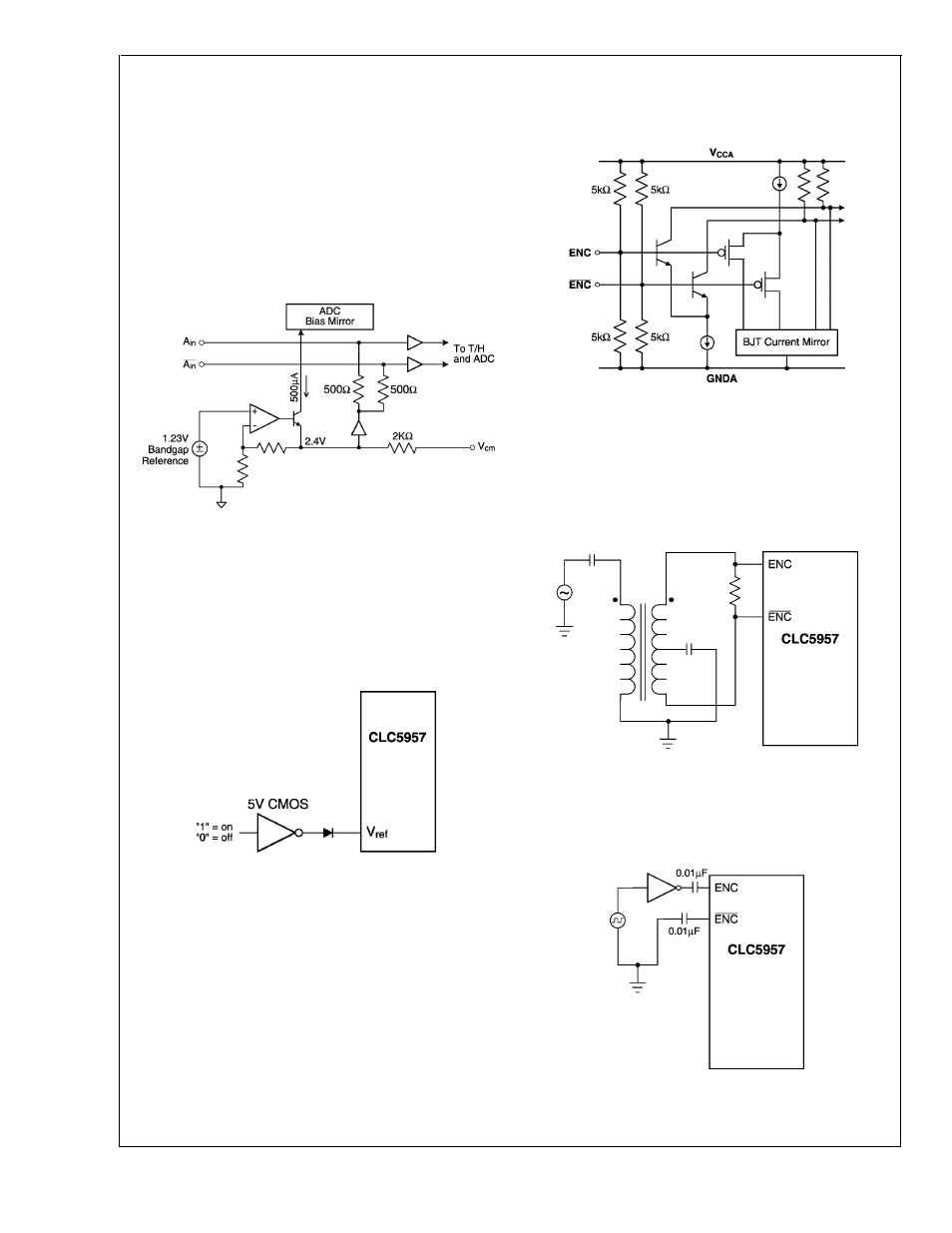
CLC5957 Applications
Analog Inputs and Bias
Figure 1 depicts the analog input and bias scheme. Each of
the differential analog inputs are internally biased to a nomi-
nal voltage of 2.40V DC through a 500
Ω
resistor to a low
impedance buffer. This enables a simple interface to a
broadband RF transformer with a center-tapped output wind-
ing that is decoupled to the analog ground. If the application
requires the inputs to be DC coupled, the V
CM
output can be
used to establish the proper common-mode input voltage for
the ADC. The V
CM
voltage reference is generated from an
internal bandgap source that is very accurate and stable.
The V
CM
output may also be used to power down the ADC.
When the V
CM
pin is pulled above 3.5V, the internal bias
mirror is disabled and the total current is reduced to less than
10mA.
Figure 2 depicts how this function can be used. The
diode is necessary to prevent the logic gate from altering the
ADC bias value.
ENCODE Clock Inputs
The CLC5957’s differential input clock scheme is compatible
with all commonly used clock sources. Although small differ-
ential and single-ended signals are adequate, for best aper-
ture jitter performance a low noise differential clock with a
high slew rate is preferred. As depicted in
Figure 3, both
ENCODE clock inputs are internally biased to V
CC
/2 through
a pair of 5k
Ω
resistors. The clock input buffer operates with
any common-mode voltage between the supply and ground.
The internal bias resistors simplify the clock interface to
another center-tapped transformer as depicted in
Figure 4. A
low
phase
noise,
RF
synthesizer
of
moderate
amplitude (1 − 4V
PP
) can drive the ADC through this inter-
face.
Figure 5 shows the clock interface scheme for square wave
clock sources.
015029F1
FIGURE 1. CLC5957 Bias Scheme
015029F2
FIGURE 2. Power Shutdown Scheme
015029F3
FIGURE 3. CLC5957 ENCODE Clock Inputs
015029F4
FIGURE 4. Transformer Coupled Clock Scheme
015029F5
FIGURE 5. TTL, 3V CMOS or 5V CMOS Clock Scheme
CLC5957
www.national.com
14