Ds2741, Applications information, Package information – Rainbow Electronics DS2741 User Manual
Page 9: Power-supply decoupling, Sda and scl pullup resistors
DS2741
Current Monitor and Accumulator with
Integrated Sense Resistor
Maxim cannot assume responsibility for use of any circuitry other than circuitry entirely embodied in a Maxim product. No circuit patent licenses are
implied. Maxim reserves the right to change the circuitry and specifications without notice at any time.
Maxim Integrated Products, 120 San Gabriel Drive, Sunnyvale, CA 94086 408-737-7600 _____________________ 9
© 2008 Maxim Integrated Products
is a registered trademark of Maxim Integrated Products, Inc.
DS2741
ble, and generates a STOP condition. See Figure 6
for a read example using the repeated START condi-
tion to specify the starting memory location.
Reading Multiple Bytes from a Slave: The read
operation can be used to read multiple bytes with a
single transfer. When reading bytes from the slave,
the master simply ACKs the data byte if it desires to
read another byte before terminating the transaction.
After the master reads the last byte, it NACKs to
indicate the end of the transfer and generates a
STOP condition. This can be done with or without
modifying the address counter’s location before the
read cycle. The DS2741’s address counter does not
wrap on page boundaries during read operations,
but the counter rolls from its uppermost memory
address FFh to 00h if the last memory location is
read during the read transaction.
Applications Information
Power-Supply Decoupling
To achieve best results, it is recommended that the power
supply is decoupled with a 0.01µF or a 0.1µF capacitor.
Use high-quality, ceramic, surface-mount capacitors, and
mount the capacitors as close as possible to the V
CC
and
GND pins to minimize lead inductance.
SDA and SCL Pullup Resistors
SDA is an open-collector output on the DS2741 that
requires a pullup resistor to realize high logic levels. A
master using either an open-collector output with a
pullup resistor or a push-pull output driver can be used
for SCL. Pullup resistor values should be chosen to
ensure that the rise and fall times listed in the AC elec-
trical characteristics are within specification.
Package Information
For the latest package outline information and land patterns, go
to
www.maxim-ic.com/packages
.
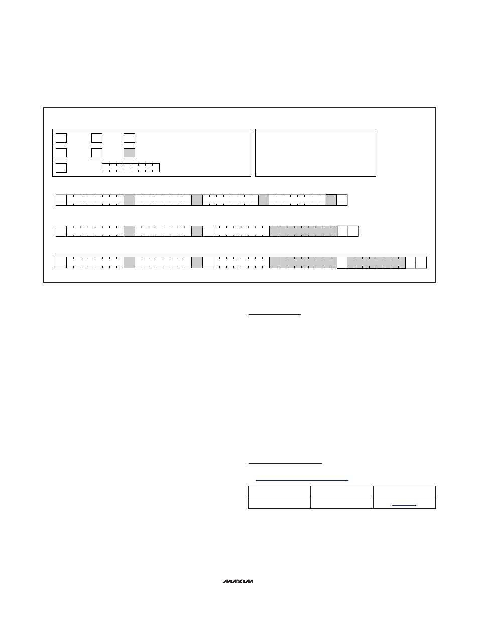
Figure 6. I
2
C Communications Examples
S
P
SR
A
N
START
8-BIT ADDRESS OR DATA
REPEATED
START
STOP
ACK
NACK
WHITE BOXES INDICATE THE MASTER IS
CONTROLLING SDA
SHADED BOXES INDICATE THE SLAVE IS
CONTROLLING SDA
COMMUNICATIONS KEY
X X X X X X X X
NOTES
1) ALL BYTES ARE SENT MOST SIGNIFICANT BIT FIRST.
2) THE FIRST BYTE SENT AFTER A START CONDITION
IS ALWAYS THE SLAVE ADDRESS FOLLOWED BY
THE READ/WRITE BIT.
WRITE TWO BYTES WITH A SINGLE TRANSACTION TO SLAVE ADRESS 68h
S
0 1 1 0
0 0
A
MEMORY ADDRESS
A
A
DATA
DATA
A
P
0
1
A
DATA
SR 0 1 1 0
0 1
A
N
P
0
1
READ A SINGLE BYTE WITH A DUMMY WRITE CYCLE TO SET THE ADDRESS COUNTER FROM SLAVE ADDRESS 68h
S
0 1 1 0
0 0
A
MEMORY ADDRESS
0
1
A
DATA
N
P
A
DATA
SR 0 1 1 0
0 1
A
0
1
READ TWO BYTES WITH A DUMMY WRITE CYCLE TO SET THE ADDRESS COUNTER FROM SLAVE ADDRESS 68h
S
0 1 1 0
0 0
A
MEMORY ADDRESS
0
1
PACKAGE TYPE
PACKAGE CODE
DOCUMENT NO.
14 TDFN-EP
T1433+2