Pin descriptions and equivalent circuits – Rainbow Electronics ADC12DL066 User Manual
Page 3
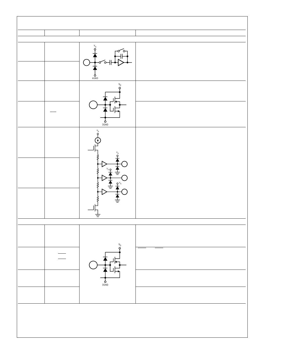
Pin Descriptions and Equivalent Circuits
Pin No.
Symbol
Equivalent Circuit
Description
ANALOG I/O
15
2
V
IN
A+
V
IN
B+
Differential analog input pins. With a 1.0V reference voltage
the differential full-scale input signal level is 2.0 V
P-P
with
each input pin voltage centered on a common mode voltage,
V
CM
. The negative input pins may be connected to V
CM
for
single-ended operation, but a differential input signal is
required for best performance.
16
1
V
IN
A−
V
IN
B−
7
V
REF
Reference input. This pin should be bypassed to AGND with
a 0.1 µF capacitor when an external reference is used. V
REF
is 1.0V nominal and should be between 0.8V to 1.5V.
11
INT/EXT REF
Reference source select pin. With a logic low at this pin the
internal 1.0V reference is selected and the V
REF
pin need
not be driven. With a logic high on this pin an external
reference voltage should be applied to V
REF
input pin 7.
13
5
V
RP
A
V
RP
B
These pins are high impedance reference bypass pins.
Bypass per Section 1.2. DO NOT LOAD these pins.
14
4
V
RM
A
V
RM
B
12
6
V
RN
A
V
RN
B
DIGITAL I/O
60
CLK
Digital clock input. The range of frequencies for this input is
as specified in the electrical tables with guaranteed
performance at 66 MHz. The input is sampled on the rising
edge of this input.
22
41
OEA
OEB
OEA and OEB are the output enable pins that, when low,
holds their respective data output pins in the active state.
When either of these pins is high, the corresponding outputs
are in a high impedance state.
59
PD
PD is the Power Down input pin. When high, this input puts
the converter into the power down mode. When this pin is
low, the converter is in the active mode.
21
OF
Output Format pin. A logic low on this pin causes output
data to be in offset binary format. A logic high on this pin
causes the output data to be in 2’s complement format.
ADC12DL066
www.national.com
3