Figure 6. example of a suitable layout, 0 dynamic performance, Applications information – Rainbow Electronics ADC12DL066 User Manual
Page 21

Applications Information
(Continued)
Be especially careful with the layout of inductors. Mutual
inductance can change the characteristics of the circuit in
which they are used. Inductors should not be placed side by
side, even with just a small part of their bodies beside each
other.
The analog input should be isolated from noisy signal traces
to avoid coupling of spurious signals into the input. Any
external component (e.g., a filter capacitor) connected be-
tween the converter’s input pins and ground or to the refer-
ence input pin and ground should be connected to a very
clean point in the ground plane.
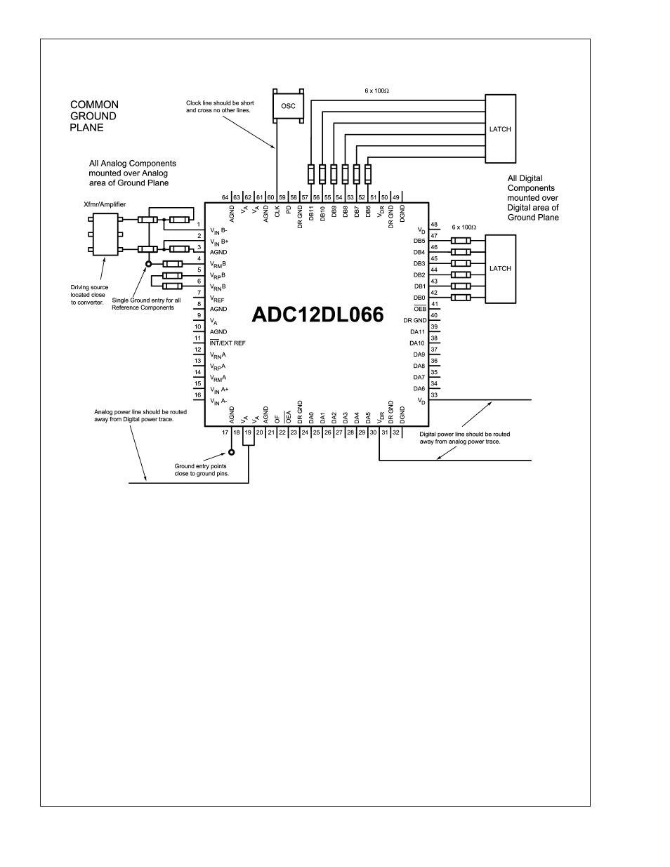
Figure 6 gives an example of a suitable layout. All analog
circuitry (input amplifiers, filters, reference components, etc.)
should be placed in the analog area of the board. All digital
circuitry and I/O lines should be placed in the digital area of
the board. The ADC12DL066 should be between these two
areas. Furthermore, all components in the reference circuitry
and the input signal chain that are connected to ground
should be connected together with short traces and enter the
ground plane at a single, quiet point. All ground connections
should have a low inductance path to ground.
6.0 DYNAMIC PERFORMANCE
To achieve the best dynamic performance, the clock source
driving the CLK input must be free of jitter. Isolate the ADC
clock from any digital circuitry with buffers, as with the clock
tree shown in Figure 7. The gates used in the clock tree must
be capable of operating at frequencies much higher than
those used if added jitter is to be prevented.
Best performance will be obtained with a differential input
drive, compared with a single-ended drive, as discussed in
Sections 1.3.1 and 1.3.2.
As mentioned in Section 5.0, it is good practice to keep the
ADC clock line as short as possible and to keep it well away
from any other signals. Other signals can introduce jitter into
the clock signal, which can lead to reduced SNR perfor-
mance, and the clock can introduce noise into other lines.
Even lines with 90˚ crossings have capacitive coupling, so
try to avoid even these 90˚ crossings of the clock line.
20055216
FIGURE 6. Example of a Suitable Layout
ADC12DL066
www.national.com
21
