Figure 4, Applications information – Rainbow Electronics ADC12DL066 User Manual
Page 19

Applications Information
(Continued)
Be very careful when driving a high capacitance bus. The
more capacitance the output drivers must charge for each
conversion, the more instantaneous digital current flows
through V
DR
and DR GND. These large charging current
spikes can cause on-chip ground noise and couple into the
analog circuitry, degrading dynamic performance. Adequate
bypassing, limiting output capacitance and careful attention
to the ground plane will reduce this problem. Additionally,
bus capacitance beyond the specified 15 pF/pin will cause
t
OD
to increase, making it difficult to properly latch the ADC
output data. The result could be an apparent reduction in
dynamic performance.
To minimize noise due to output switching, minimize the load
currents at the digital outputs. This can be done by connect-
ing buffers (74ACQ541, for example) between the ADC out-
puts and any other circuitry. Only one driven input should be
connected to each output pin. Additionally, inserting series
resistors of about 100
Ω at the digital outputs, close to the
ADC pins, will isolate the outputs from trace and other circuit
capacitances and limit the output currents, which could oth-
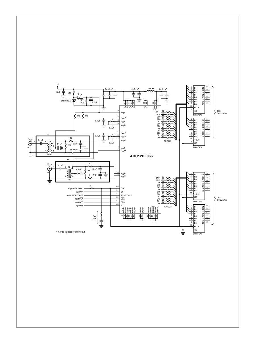
erwise result in performance degradation. See Figure 4.
20055213
FIGURE 4. Application Circuit using Transformer or Differential Op-Amp Drive Circuit
ADC12DL066
www.national.com
19
