Clock and calendar, Figure 6. rtc and ram address map – Rainbow Electronics DS1338 User Manual
Page 10
DS1338 I
2
C RTC with 56-Byte NV RAM
10 of 15
CLOCK AND CALENDAR
The time and calendar information is obtained by reading the appropriate register bytes. See Figure 6 for the RTC
registers. The time and calendar are set or initialized by writing the appropriate register bytes. The contents of the
time and calendar registers are in the BCD format. Bit 7 of Register 0 is the clock halt (CH) bit. When this bit is set
to 1, the oscillator is disabled. When cleared to 0, the oscillator is enabled. The clock can be halted whenever the
timekeeping functions are not required, which decreases V
BAT
current.
The day-of-week register increments at midnight. Values that correspond to the day of week are user-defined but
must be sequential (i.e., if 1 equals Sunday, then 2 equals Monday, and so on). Illogical time and date entries
result in undefined operation.
When reading or writing the time and date registers, secondary (user) buffers are used to prevent errors when the
internal registers update. When reading the time and date registers, the user buffers are synchronized to the
internal registers on any start or stop and when the register pointer rolls over to zero. The countdown chain is reset
whenever the seconds register is written. Write transfers occur on the acknowledge from the DS1338. Once the
countdown chain is reset, to avoid rollover issues the remaining time and date registers must be written within
1 second. The 1Hz square-wave output, if enabled, transitions high 500ms after the seconds data transfer,
provided the oscillator is already running.
Note that the initial power-on state of all registers, unless otherwise specified, is not defined. Therefore, it
is important to enable the oscillator (CH = 0) during initial configuration.
The DS1338 runs in either 12-hour or 24-hour mode. Bit 6 of the hours register is defined as the 12-hour or 24-hour
mode-select bit. When high, the 12-hour mode is selected. In the 12-hour mode, bit 5 is the
AM/PM bit, with logic
high being PM. In the 24-hour mode, bit 5 is the second 10-hour bit (20–23 hours). If the 12/
24-hour mode select is
changed, the hours register must be re-initialized to the new format.
On an I
2
C START, the current time is transferred to a second set of registers. The time information is read from
these secondary registers, while the clock continues to run. This eliminates the need to re-read the registers in
case of an update of the main registers during a read.
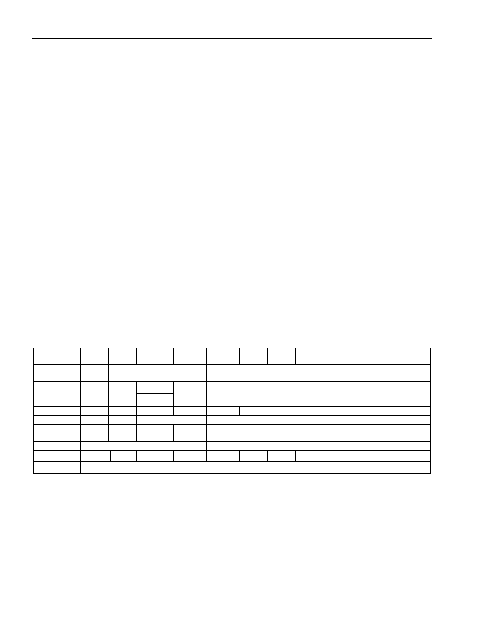
Figure 6. RTC and RAM Address Map
ADDRESS
BIT 7
BIT 6
BIT 5
BIT 4
BIT 3
BIT 2
BIT 1
BIT 0
FUNCTION
RANGE
00H CH
10
Seconds
Seconds
Seconds 00–59
01H 0
10
Minutes
Minutes
Minutes 00–59
AM/PM
02H 0
12/
24
10 Hour
10
Hour
Hour Hours
1–12
+AM/PM
00–23
03H 0
0 0 0 0
Day
Day
1–7
04H 0
0 10
Date
Date
Date 01–31
05H 0
0 0
10
Month
Month Month
01–12
06H 10
Year
Year Year
00–99
07H OUT
0 OSF
SQWE
0 0
RS1
RS0 Control
08H–3FH
RAM 56 x 8
00H–FFH
Note: Bits listed as “0” always read as a 0.