Icl7665, Detailed description – Rainbow Electronics ICL7665 User Manual
Page 6
ICL7665
_______________Detailed Description
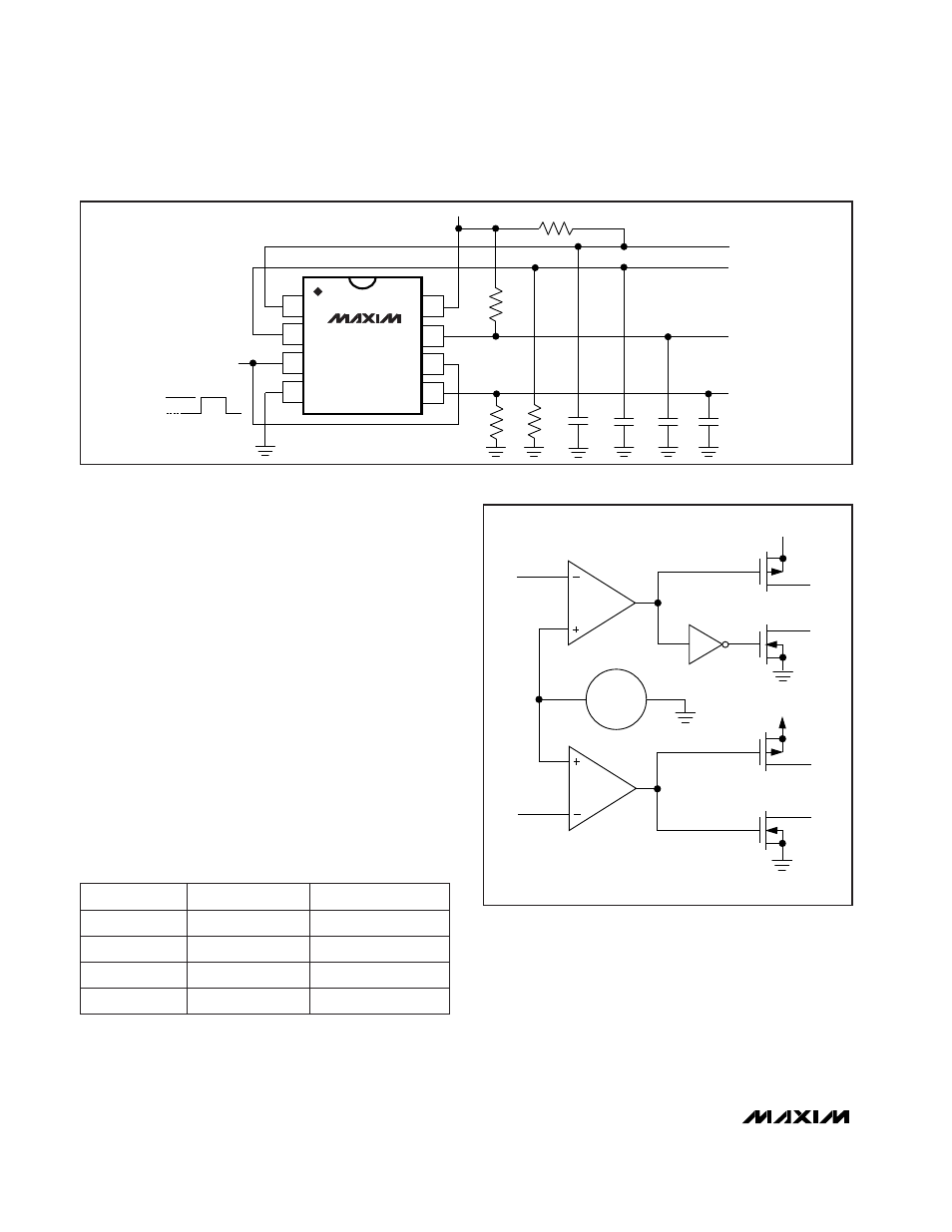
As shown in the block diagram of Figure 2, the Maxim
ICL7665 combines a 1.3V reference with two com-
parators, two open-drain N-channel outputs, and two
open-drain P-channel hysteresis outputs. The refer-
ence and comparator are very low-power linear CMOS
circuits, with a total operating current of 10
µ
A maxi-
mum, 3
µ
A typical. The N-channel outputs can sink
greater than 10mA, but are unable to source any cur-
rent. These outputs are suitable for wire-OR connections
and are capable of driving TTL inputs when an external
pull-up resistor is added.
The ICL7665 Truth Table is shown in Table 1. OUT1 is
an inverting output; all other outputs are noninverting.
HYST1 and HYST2 are P-channel current sources
whose sources are connected to V+. OUT1 and OUT2
are N-channel current sinks with their sources connect-
ed to ground. Both OUT1 and OUT2 can drive at least
one TTL load with a V
OL
of 0.4V.
In spite of the very low operating current, the ICL7665
has a typical propagation delay of only 75
µ
s. Since the
comparator input bias current and the output leakages
are very low, high-impedance external resistors can be
used. This design feature minimizes both the total sup-
ply current used and loading on the voltage source that
is being monitored.
Microprocessor Voltage Monitor with
Dual Over/Undervoltage Detection
6
_______________________________________________________________________________________
Figure 1. Test Circuit
HYST2 = OFF = LOW
OUT2 = ON = LOW
V
SET2
< 1.3V
HYST2 = ON = HI
OUT2 = OFF = HI
V
SET2
> 1.3V
HYST1 = OFF = LOW
OUT1 = OFF = HI
V
SET1
< 1.3V
HYST1 = ON = HI
OUT1 = ON = LOW
V
SET1
> 1.3V
HYSTERESIS
OUTPUT
INPUT*
Table 1. ICL7665 Truth Table
V+
HYST1
HYST2
OUT1
OUT2
TO V+
SET2
SET1
1.3V
BANDGAP
REFERENCE
Figure 2. Block Diagram
1
2
3
4
8
7
6
5
ICL7665
OUT1
HYST1
SET1
GND
V+
OUT2
SET2
HSYT2
12pF
12pF
12pF
12pF
OUT1
HYST1
OUT2
HSYT2
4.7k
4.7k
V+
1.6V
1.0V
INPUT
20k
20k
* See Electrical Characteristics
OUT1 is an inverting output; all others are noninverting. OUT1
and OUT2 are open-drain, N-channel current sinks. HYST1
and HYST2 are open-drain, P-channel current sinks.