Rainbow Electronics ICL7665 User Manual
Page 2
ICL7665
Microprocessor Voltage Monitor with
Dual Over/Undervoltage Detection
2
_______________________________________________________________________________________
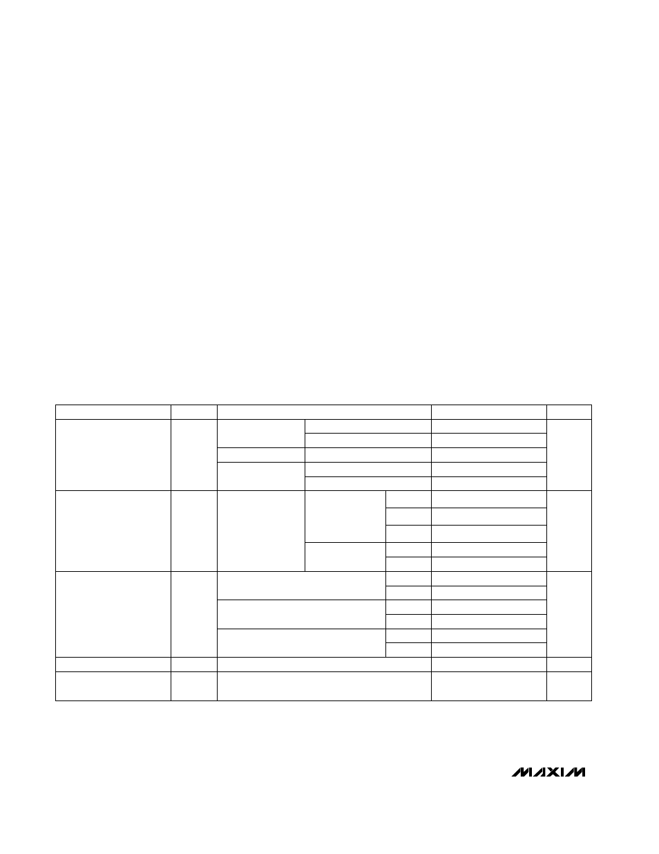
ABSOLUTE MAXIMUM RATINGS
ELECTRICAL CHARACTERISTICS
(V+ = 5V, T
A
= +25°C, unless otherwise noted.)
Stresses beyond those listed under “Absolute Maximum Ratings” may cause permanent damage to the device. These are stress ratings only, and functional
operation of the device at these or any other conditions beyond those indicated in the operational sections of the specifications is not implied. Exposure to
absolute maximum rating conditions for extended periods may affect device reliability.
Note 1:
Due to the SCR structure inherent in the CMOS process used to fabricate these devices, connecting any terminal to volt-
ages greater than (V+ + 0.3V) or less than (GND - 0.3V) may cause destructive latchup. For this reason, we recommend
that inputs from external sources that are not operating from the same power supply
not
be applied to the device before its
supply is established, and that in multiple supply systems, the supply to the ICL7665 be turned on first. If this is not possi-
ble, currents into inputs and/or outputs must be limited to ±0.5mA and voltages must not exceed those defined above.
Supply Voltage (Note 1) .........................................-0.3V to +18V
Output Voltages OUT1 and OUT2
(with respect to GND) (Note 1) ..........................-0.3V to +18V
Output Voltages HYST1 and HYST2
(with respect to V+) (Note 1) .............................+0.3V to -18V
Input Voltages SET1 and SET2
(Note 1)........................................(GND - 0.3V) to (V+ + 0.3V)
Maximum Sink Output Current
OUT1 and OUT2.............................................................25mA
Maximum Source Output Current
HYST1 and HYST2 ........................................................-25mA
Continuous Power Dissipation (T
A
= +70°C)
Plastic DIP (derate 9.09mW/°C above +70°C) ............727mW
SO (derate 5.88mW/°C above +70°C) ........................471mW
CERDIP (derate 8.00mW/°C above +70°C) ................640mW
TO-99 (derate 6.67mW/°C above +70°C) ...................533mW
Operating Temperature Ranges
ICL7665C_ _.......................................................0°C to +70°C
ICL7665I_ _ .....................................................-20°C to +85°C
ICL7665E_ _ ....................................................-40°C to +85°C
Storage Temperature Range .............................-65°C to +160°C
Lead Temperature (soldering, 10sec) .............................+300°C
PARAMETER
SYMBOL
CONDITIONS
MIN
TYP
MAX
UNITS
Operating Supply Voltage
V+
ICL7665
T
A
= +25°C
1.6
16
V
T
A
= T
MIN
to T
MIN
1.8
16
ICL7665A
T
A
= T
MIN
to T
MIN
2.0
16
ICL7665B
T
A
= +25°C
1.6
10
Input Trip Voltage
V
SET
ICL7665, ICL7665B, T
A
= +25°C
V
SET1
1.150
1.300
1.450
V
V
SET2
1.200
1.300
1.400
ICL7665A, T
A
= +25°C
V
SET1
1.275
1.300
1.325
V
SET2
1.225
1.300
1.375
ICL7665A, T
A
= T
MIN
to T
MAX
V
SET1
1.250
1.300
1.350
V
SET2
1.215
1.300
1.385
V
SET
Tempco
100
ppm/°C
R
OUT1
, R
OUT2
, R
HYST1
, R
HYST2
= 1M
Ω
0.004
%/V
Supply Current
I+
GND
≤
V
SET1,
V
SET2
≤
V+,
all outputs open
circuit
V+ = 2V
2.5
10
µ
A
V+ = 9V
2.6
10
V+ = 15V
2.9
15
ICL7665B,
T
A
= +25°C
V+ = 2V
2.5
10
V+ = 9V
2.6
10
T
A
= T
MIN
to T
MIN
1.8
10
ICL7665,
T
A
= +25°C;
ICL7665A,
T
A
= T
MIN
to T
MAX
Supply Voltage Sensitivity
of V
SET1
, V
SET2