Marking lot.no, And resistance r, Part number and marking of samples – Rainbow Electronics BD4719G User Manual
Page 4

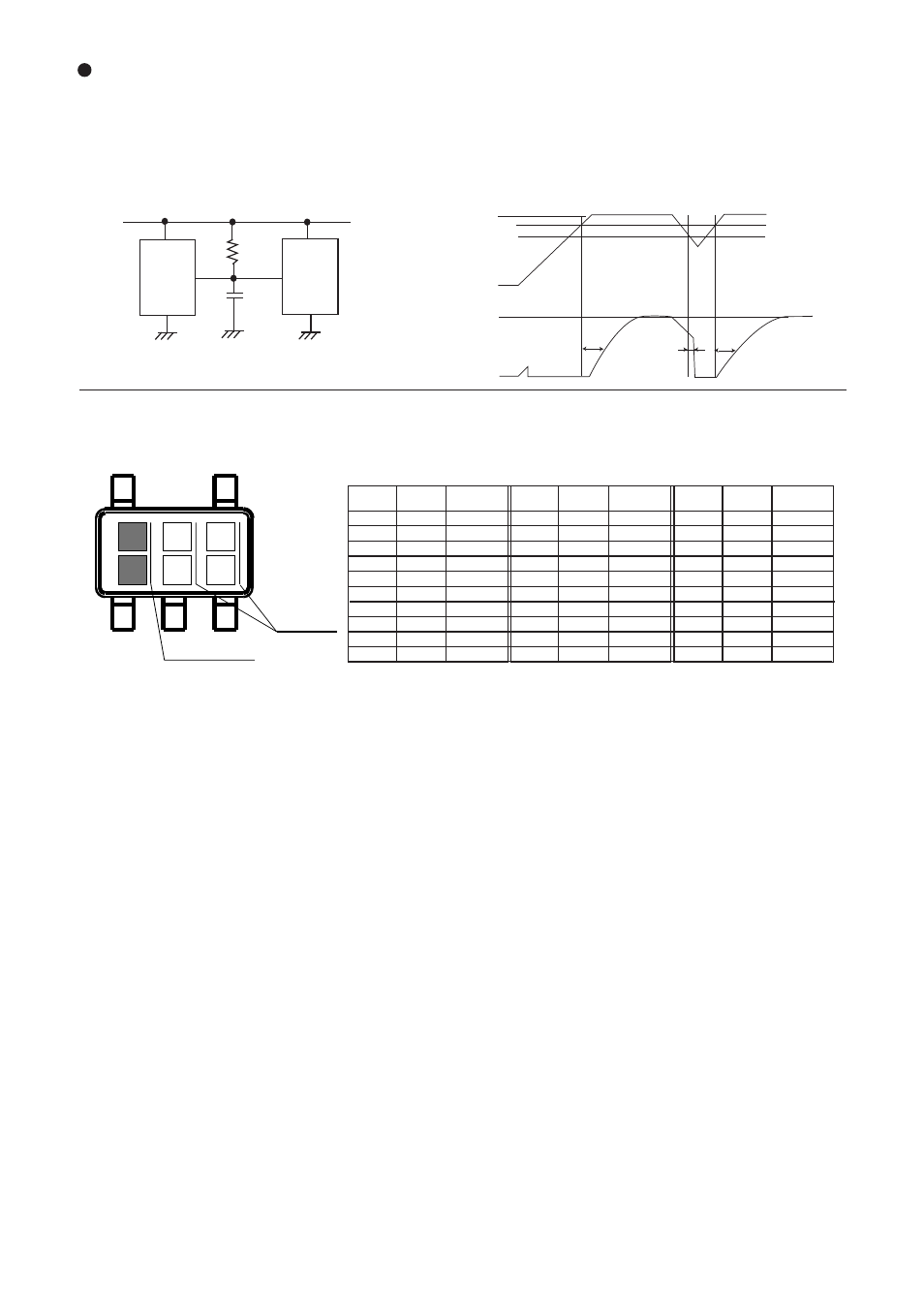
Setting of the RESET signal delay time
Delay time can be set by capacitor C
L
and resistance R
L
connected to the output pin as shown below.
CL is charged by R
L
when Vcc is rising. The delay time caused by charging is determined by the
time constant of C
L
, R
L
and the threshold voltage of RESET pin. RESET IC discharges C
L
forcedly
when Vcc is falling. The delay time of RESET signal is determined by adding the delay time of single
RESET IC to each time.
GND
GND
Vcc
V
DD
C
L
Vout
RESET
BD47XXG
CPU
Micro-controller
R
L
VCC
VCC
RESET
(=VOUT)
VS
0V
VOH
T
PLH
T
PLH
VOL
VS+
∆VS
T
PHL
Marking
Voltage
Part No.
Part No.
Part No.
Marking
Marking
Voltage
Voltage
BD4719
BA
BB
BC
BD
BE
BF
BG
BH
B3
BJ
1.9V
2.0V
2.1V
2.2V
2.3V
2.4V
2.5V
2.6V
2.7V
2.8V
BK
BL
BM
BN
B4
BP
BQ
BR
BS
BT
2.9V
3.0V
3.1V
3.2V
3.3V
3.4V
3.5V
3.6V
3.7V
3.8V
BU
BV
BW
BX
BY
BZ
B1
B2
3.9V
4.0V
4.1V
4.2V
4.3V
4.4V
4.5V
4.6V
BD4729
BD4720
BD4721
BD4722
BD4723
BD4724
BD4725
BD4726
BD4727
BD4728
BD4730
BD4731
BD4732
BD4733
BD4734
BD4735
BD4736
BD4737
BD4738
BD4739
BD4740
BD4741
BD4742
BD4743
BD4744
BD4745
BD4746
Part number and Marking of samples
(5)
(4)
(3)
(2)
(1)
Marking
Lot.No
