Fig.4 maximum output voltage vs. frequency, Fig.5 input bias current vs. ambient temperature, Fig.6 input bias current vs. power supply voltage – Rainbow Electronics BA10324AFV User Manual
Page 4: Fig.8 output voltage vs. output sink current, Fig.9 output response characteristics, Fig.10 unused circuit connections
4
Standard ICs
BA10324A / BA10324AF / BA10324AFV
20
15
10
5
0
100
1k
10k
100k
1M
FREQUENCY: f (Hz)
MAXIMUM OUTPUT VOLTAGE: V
OM
(V)
100k
V
O
V
IN
2k
1k
7V
15V
~
+
–
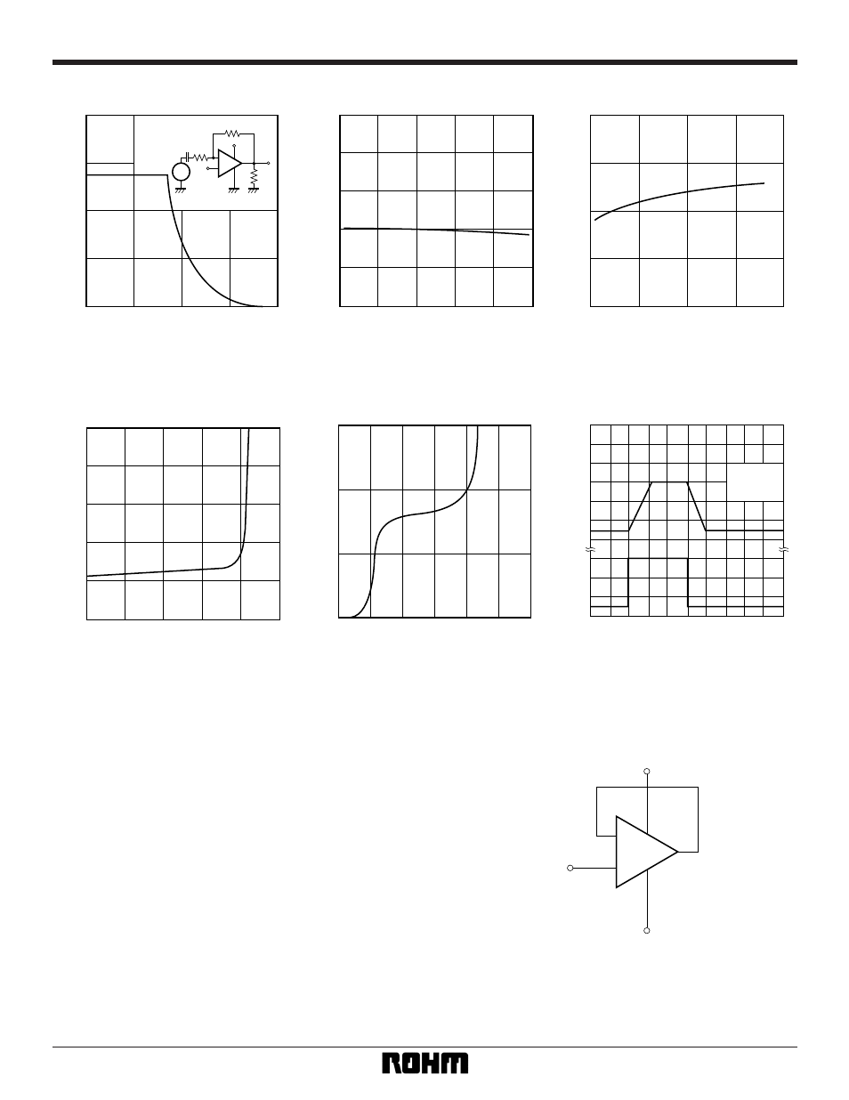
Fig.4 Maximum output voltage vs.
frequency
50
40
0
– 20
0
20
40
60
80
10
20
30
AMBIENT TEMPERATURE: Ta (
°
C)
INPUT BIAS CURRET
:
I
B
(
nA)
Fig.5 Input bias current vs. ambient
temperature
40
0
10
20
30
40
10
20
30
POWER SUPPLY VOLTAGE: V
+
(V)
INPUT BIAS CURRENT: I
B
(nA)
Fig.6 Input bias current vs. power supply
voltage
5
3
2
4
0
0.001
0.01
0.1
1.0
10
100
1
OUTPUT SOURCE CURRENT (mA)
OUTPUT VOLTAGE
REFERENCED TO V
+
:
∆
V (V)
Fig.7 Potential difference during
power supply output vs. output
source current
0.01
0.1
1.0
10
0.001
0.01
0.1
1.0
10
100
1000
OUTPUT SINK CURRENT: I
O
(mA)
OUTPUT VOLTAGE: V
O
(V)
Fig.8 Output voltage vs. output sink
current
R
L
м
2k
Ω
V
CC
= 15V
4
3
2
1
0
0
0
20
40
60
80
1
2
3
TIME (
µ
s)
INPUT VOLTAGE OUTPUT VOLTAGE
V
IN
(V) V
OUT
(V)
Fig.9 Output response characteristics
•
Operation notes
(1) Unused circuit connections
If there are any circuits which are not being used, we
recommend making connections as shown in Figure
10, with the non-inverted input pin connected to the
potential within the in-phase input voltage range (V
ICM
).
V
CC
V
EE
+
–
Fig.10 Unused circuit connections
To potential
in V
ICM