Block diagram/typical application circuit, Detailed description – Rainbow Electronics DS4560 User Manual
Page 5
DS4560
THERMAL
LIMIT
EXTERNAL DISABLE
TIMER
C
TIMER
+5V
2.5V
UVLO
CURRENT
LIMIT
CHARGE
PUMP
LOAD
+5V
VREG
OVERVOLTAGE
LIMIT
GND
R
R
R
ILIM
LOAD
ILIM
+12V
V
CC
VRAMP
V
CC
80
μA
80
μA
C
VRAMP
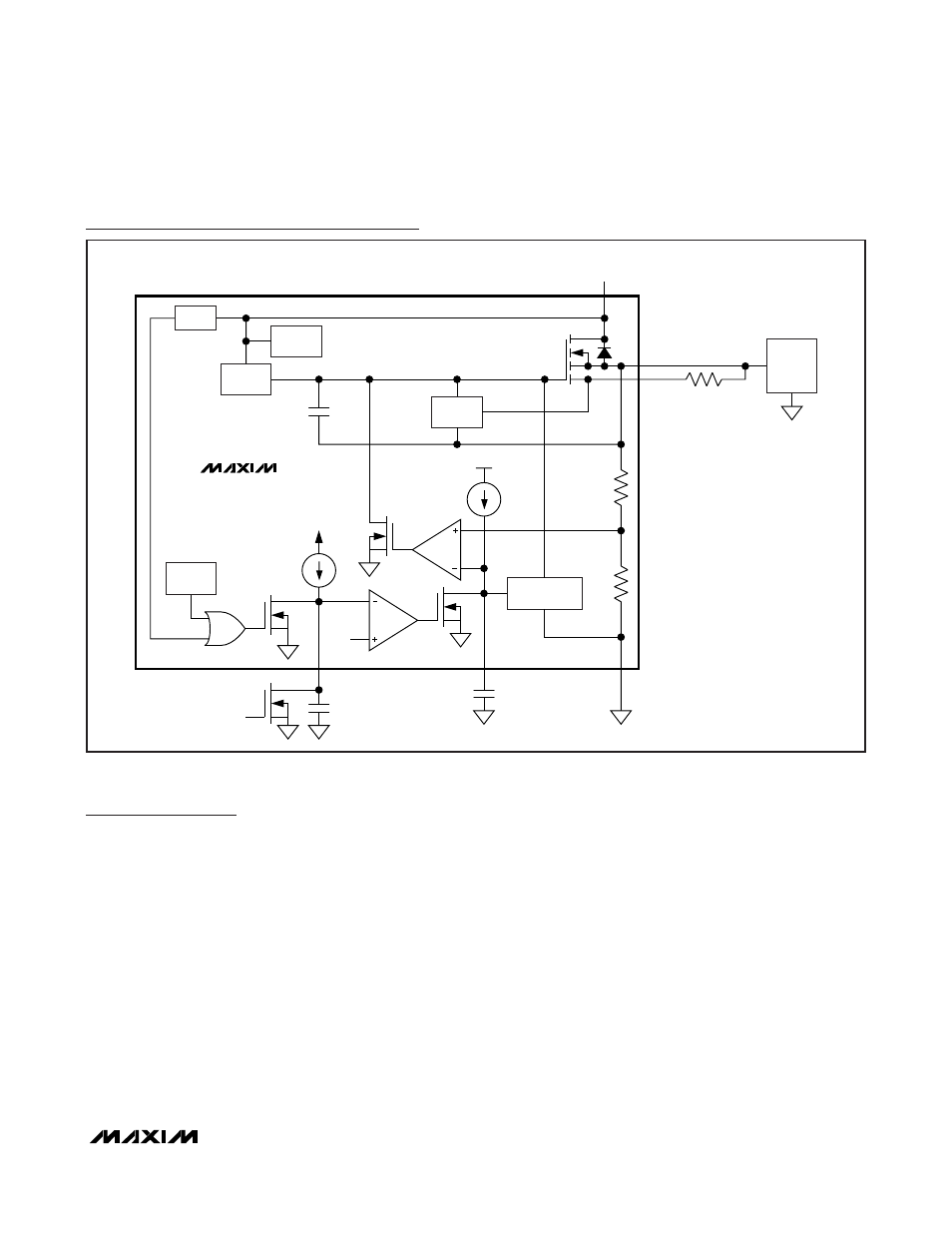
Block Diagram/Typical Application Circuit
DS4560
12V Hot-Plug Switch
_______________________________________________________________________________________
5
Detailed Description
The DS4560 begins to operate when V
CC
exceeds the
undervoltage lockout level, V
UVLOR
. At this level, the
enable circuit and TIMER pin become active. Once the
device has been enabled, a gate voltage is applied to
the power MOSFET, allowing current to begin flowing
from V
CC
to LOAD. The speed of the output-voltage
ramp is controlled by the capacitance placed at the
VRAMP pin. The load current is continuously monitored
during the initial voltage ramping (I
SCL
) and during nor-
mal operation (I
OVL
). If the current exceeds the current
limit that is set by the external resistance at ILIM, the
gate voltage of the power MOSFET is decreased,
reducing the output current to the set current limit.
Current is limited by the DS4560 comparing the voltage
difference between the LOAD and ILIM pins to an inter-
nal reference voltage. If the output current exceeds the
limit that is set by the R
ILIM
resistor, the gate voltage of
the power MOSFET is decreased, which reduces the
output current to the load.
When the output power is initially ramping up, the current
limit is I
SCL
. Once the voltage ramping is complete, the
current limit is I
OVL
. The lower I
SCL
current limit protects
the source if there is a dead short on initial power-up.
The DS4560 acts as a fuse and automatically disables
the current flowing to the load when the temperature of
the power MOSFET has exceeded the shutdown junc-
tion temperature, T
SHDN
.