Electrical characteristics – Rainbow Electronics DS4560 User Manual
Page 2
DS4560
12V Hot-Plug Switch
2
_______________________________________________________________________________________
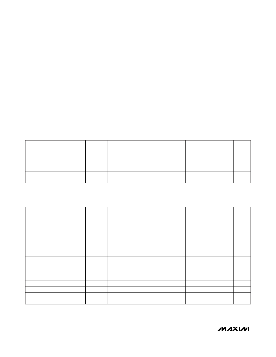
ABSOLUTE MAXIMUM RATINGS
RECOMMENDED OPERATING CONDITIONS
(T
J
= -40°C to +135°C.)
Stresses beyond those listed under “Absolute Maximum Ratings” may cause permanent damage to the device. These are stress ratings only, and functional
operation of the device at these or any other conditions beyond those indicated in the operational sections of the specifications is not implied. Exposure to
absolute maximum rating conditions for extended periods may affect device reliability.
Voltage Range on V
CC
and LOAD Relative to GND
Continuous .........................................................-0.3V to +18V
1ms Maximum ....................................................-0.3V to +22V
Voltage Range on ILIM and VRAMP
Relative to GND.....................................-0.3V to (V
CC
+ 0.3V),
but not to exceed +18V
Voltage Range on TIMER Relative to GND ...........-0.3V to +5.0V
Drain Current
Continuous ...........................................................................4A
Peak ...................................................................................15A
Operating Junction Temperature Range ...........-40
°C to +135°C
Storage Temperature Range .............................-55
°C to +135°C
Soldering Temperature...........................Refer to the IPC/JEDEC
J-STD-020 Specification.
PARAMETER
SYMBOL
CONDITIONS
MIN
TYP
MAX
UNITS
Supply Voltage
V
CC
(Notes 1, 2)
9.0
13.2
V
R
ILIM
Value
R
ILIM
20
400
C
VRAMP
Value
C
VRAMP
0.04
5.00
μF
C
TIMER
Value C
TIMER
0.04
5.00
μF
TIMER Turn-On Voltage
V
ON
2.6
5
V
TIMER Turn-Off Voltage
V
OFF
-0.3
+2.0 V
ELECTRICAL CHARACTERISTICS
(V
CC
= +12V, T
J
= +25°C, unless otherwise noted.)
PARAMETER
SYMBOL
CONDITIONS
MIN
TYP
MAX
UNITS
Supply Current
I
CC
(Note
3)
1.1 2.00 mA
UVLO Rising
V
UVLOR
7.5 8.0 8.5 V
UVLO Falling
V
UVLOF
6.5 7.0 7.5 V
UVLO Hysteresis
V
UVLOH
1 V
On-Resistance R
ON
25 32 m
MOSFET Output Capacitance
C
OUT
500
pF
LOAD Voltage During Off State
V
LOFF
(Note
4)
200 mV
Delay Time from Enable to
Beginning of Conduction
t
POND
C
VRAMP
=
1μF
5 ms
Gate-Charging Time from
Conduction to 90% of V
OUT
t
GCT
C
VRAMP
= 1μF, C
LOAD
=
1000μF
48 66 80 ms
Shutdown Junction Temperature
T
SHDN
(Note
5)
120 135 150 °C
Thermal Hysteresis
T
HYS
(Note
5)
40 °C
TIMER Charging Current
I
TIMER
70 80 92 μA
Overvoltage Clamp
V
OVC
13.5 15.0 16.5 V