Ds7505 digital thermometer and thermostat, Ac electrical characteristics (continued) – Rainbow Electronics DS7505 User Manual
Page 3
DS7505
Digital Thermometer and Thermostat
_______________________________________________________________________________________
3
Note 1:
All voltages are referenced to ground.
Note 2:
Internal heating caused by O.S. loading causes the DS7505 to read approximately 0.5°C higher if O.S. is sinking the
max-rated current.
Note 3:
Specified in 12-bit conversion mode. Quantization error must be considered when converting in lower resolutions.
Note 4:
I
DD
specified with O.S. pin open.
Note 5:
I
DD
specified with V
DD
at 3.0V and SDA, SCL = 3.0V, T
A
= -55°C to +85°C.
Note 6:
I
DD
specified with A0, A1, A2 = 0V or V
DD
.
Note 7:
V
DD
must be > 2.0V.
Note 8:
E
2
Copy occurs at +25°C.
Note 9:
See the timing diagram (Figure 1). All timing is referenced to 0.9 x V
DD
and 0.1 x V
DD
.
Note 10: After this period, the first clock pulse is generated.
Note 11: The DS7505 provides an internal hold time of at least 75ns on the SDA signal to bridge the undefined region of SCL’s
falling edge.
Note 12: For example, if C
B
= 300pF, then t
R(MIN)
= t
F(MIN)
= 50ns.
Note 13: This timeout applies only when the DS7505 is holding SDA low. Other devices can hold SDA low indefinitely and the
DS7505 does not reset.
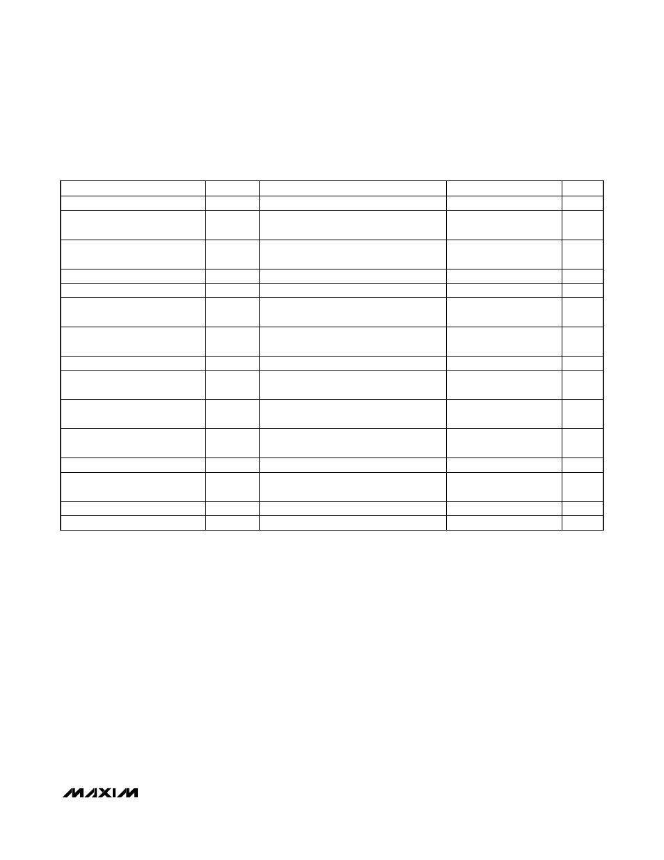
AC ELECTRICAL CHARACTERISTICS (continued)
(1.7V
≤ V
DD
≤ 3.7V, T
A
= -55°C to +125°C, unless otherwise noted.)
PARAMETER
SYMBOL
CONDITIONS
MIN
TYP
MAX
UNITS
EEPROM Data Retention
t
EEDR
-40°C to +125°C (Note 8)
10
Years
Bus Free Time Between a STOP
and START Condition
t
BUF
(Note
9)
1.3
μs
START and Repeated START
Hold Time from Falling SCL
t
HD:STA
(Notes 9, 10)
600
ns
Low Period of SCL
t
LOW
(Note
9)
1.3
μs
High Period of SCL
t
HIGH
(Note
9)
0.6
μs
Repeated START Condition
Setup Time to Rising SCL
t
SU:STA
(Note 9)
600
ns
Data-Out Hold Time from Falling
SCL
t
HD:DAT
(Notes 9, 11)
0
0.9
μs
Data-In Setup Time to Rising
t
SU:DAT
(Note 9)
100
ns
Rise Time of SDA and SCL
(Receive)
t
R
(Notes 9, 12)
20 +
0.1C
B
300
ns
Fall Time of SDA and SCL
(Receive)
t
F
(Notes 9, 12)
20 +
0.1C
B
300 ns
Spike Suppression Filter Time
(Deglitch Filter)
t
SS
0
50 ns
STOP Setup Time to Rising SCL
t
SU:STO
(Note 9)
600
ns
Capacitive Load for Each Bus
Line
C
B
400 pF
Input Capacitance
C
I
5 pF
Serial Interface Reset Time
t
TIMEOUT
SDA time low (Note 13)
75
325
ms