Voltage detectors bd45xxxg bd46xxxg, Absolute maximum ratings (ta=25˚c), Electrical characteristics – Rainbow Electronics BD46232G User Manual
Page 2: Characteristic diagram and measurement circuit
2/4
Voltage detectors
BD45XXXG
BD46XXXG
Absolute Maximum Ratings (Ta=25˚C)
Power dissipation:SSOP5
Operating temperature range
ER pin input voltage
Parameter
Symbol
Unit
Pd
Topr
V
V
mW
Storage temperature range
Tstg
Limits
– 40 ~ + 105
– 55 ~ + 125
540
V
CT
GND – 0.3 ~ + 10
V
OUT
GND – 0.3 ~ V
DD
+ 0.3
GND – 0.3 ~ V
DD
+ 0.3
˚C
˚C
V
DD
– GND
– 0.3 ~ + 10
V
∗
1
Electrical characteristics (
Unless otherwise noted; Ta=-25˚C ~ +105˚C)
V
DET
X0.03
—
—
—
—
V
DET
X0.05
0.80
0.80
0.85
—
V
DET
X0.08
2.40
—
0.70
2.10
V
DET
=2.3~3.1V
—
0.75
2.25
V
DET
=3.2~4.2V
V
DET
=4.3~4.8V
V
DET
=3.2~4.2V
V
DET
=4.3~4.8V
—
0.75
V
DET
=2.3~3.1V
2.25
2.40
2.55
0.1
µ
A
µ
A
µ
A
Icc1
Icc2
Ilaek
%
∆
V
DET
R
L
=470KΩ, V
DD
=L→H→L
Ta=-40˚C ~ +105˚C
∗
1
∗
1
∗
1
∗
1
∗
1
∗
1
∗
1
V
DET
/∆T
—
±
100
±
360
ppm/˚C
V
DD
=V
DET
–0.2V
R
L
=100kΩ
C
L
=100pF
V
DD
=V
DET
+2V
0.95
—
—
V
V
OPL
R
L
=470kΩ, V
OL
≥
0.4V
V
DD
=V
DS
=10V
1.0
2.2
—
1.2
2.7
—
mA
I
OH
V
DS
=0.5V, V
DD
=4.8V V
DET
=2.3~4.2V
V
DS
=0.5V, V
DD
=6.0V V
DET
=4.3~4.8V
2.0
5
—
mA
I
OL
0.4
1.2
—
V
DS
=0.5V, V
DD
=1.2V
V
DS
=0.5V, V
DD
=2.4V (V
DET
≥
2.7V)
—
—
0.8
V
EL
∗
1
2.0
—
—
V
EH
180
200
220
90
100
110
V
V
V
—
1
10
I
ER
V
ER
=2.0V
µ
A
t
PLH
45
50
55
BD45XX2G, BD46XX2G
BD45XX1G, BD46XX1G
BD45XX5G, BD46XX5G
Symbol
Min.
Max.
Unit
Conditions
Typ.
Parameter
Output
voltage
Power supply voltage
∗
1
Derating: 5.4mW/
˚C
for operation above Ta=25
˚C
.(Mounted on a 70.0mmX70.0mmX16mm glass epoxy PCB.)
Circuit current when ON
Circuit current when OFF
Output leak current
ER pin "H" voltage
ER pin "L" voltage
ER pin input current
"H" transmission
delay time
Hysteresis voltage
Detection voltage
temperature coefficient
Min. operating voltage
"H" output current
"L" output current
∗
1 This value is guranteed at Ta=25˚C.
Note) R
L
is not necessary for CMOS output type.
Note) Please refer to the detection voltage of Line-up table.
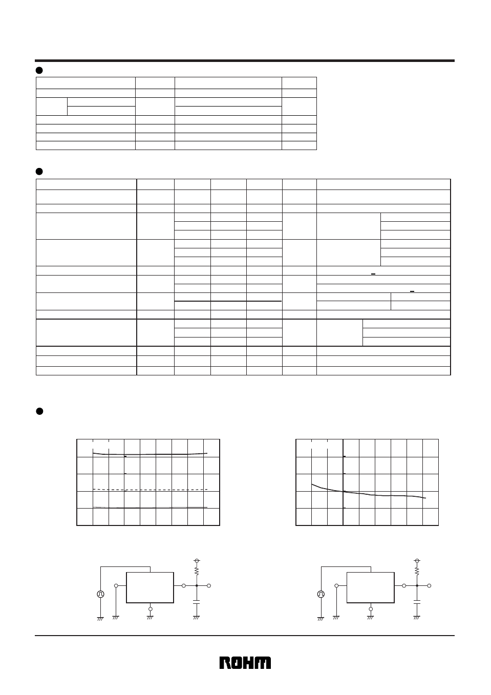
Characteristic diagram and Measurement circuit
5V
V
DET
±
0.5V
R
L
=100kΩ
100pF
V
DD
V
OUT
ER
GND
100pF
5V
V
DET
±
0.5V
R
L
=100kΩ
V
DD
V
OUT
GND
ER
Ta
(°C)
t
PL
H
(m
se
c)
250
200
150
100
50
0
-60
-40
-20
20
40
60
80
100
120
0
(BD4x28xG t
PLH
)
BD45282G
BD45281G
BD45285G
Ta
(°C)
t
PL
H
[µ
se
c]
50
40
30
20
10
0
-60
-40
-20
20
40
60
80
100
120
0
(BD4x28x t
PLH
)
Output delay time "L
→
H"
Output delay time "H
→
L"
Nch open drain output
CMOS output