Absolute maximum ratings, Dc electrical characteristics (v, 7v to 5.5v; t – Rainbow Electronics DS1726 User Manual
Page 3
DS1626/DS1726
3 of 13
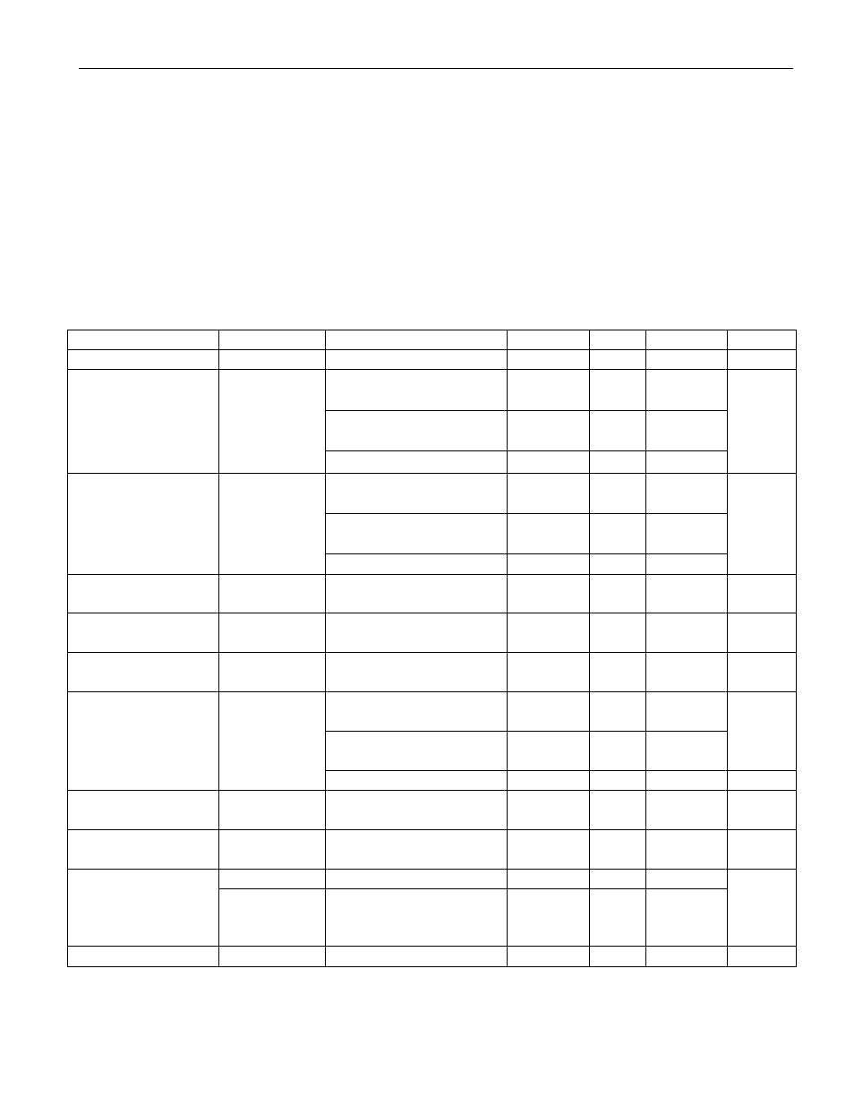
ABSOLUTE MAXIMUM RATINGS*
Voltage on Any Pin Relative to Ground
-0.5V to +6.0V
Operating Temperature Range
-55°C to +125°C
Storage Temperature Range
-55°C to +125°C
Solder Dip Temperature (10s)
+260°C
Reflow Oven Temperature
+220°C
* These are stress ratings only and functional operation of the device at these or any other conditions
above those indicated in the operation sections of this specification is not implied. Exposure to absolute
maximum rating conditions for extended periods of time may affect reliability.
DC ELECTRICAL CHARACTERISTICS
(V
DD
= 2.7V to 5.5V; T
A
= -55°C to +125°C.)
PARAMETER
SYMBOL
CONDITIONS
MIN
TYP
MAX
UNITS
Supply Voltage
V
DD
(Note 1)
2.7
5.5
V
0°C to +70°C,
3.0V
£ V
DD
£ 5.5V
±0.5
0°C to +70°C,
2.7V
£ V
DD
< 3.0V
±1.25
DS1626
Thermometer Error
(Note 2)
T
ERR
-55°C to +125°C
±2
°C
-10°C to +85°C,
3.0V
£ V
DD
£ 5.5V
±1
-10°C to +85°C,
2.7V
£ V
DD
< 3.0V
±1.5
DS1726
Thermometer Error
(Note 2)
T
ERR
-55°C to +125°C
±2
°C
Low-Level Input
Voltage
V
IL
(Note 1)
-0.5
0.3 x V
DD
V
High-Level Input
Voltage
V
IH
(Note 1)
0.7 x V
DD
V
DD
+ 0.3
V
Input Current each
Input Pin
0.4 < V
I/O
< 0.9 x V
DD
-10
+10
µA
Temperature conversion
-55°C to +85°C
1
Temperature conversion
+85°C to +125°C
1.25
mA
Active Supply
Current (Note 3)
I
DD
E
2
write
400
µA
Input Resistance
R
I
RST to GND
DQ, CLK to V
DD
1
M
W
Standby Supply
Current
I
STBY
0°C to +70°C (Note 3)
1.5
µA
V
OH
1mA source current
2.4
THIGH, TLOW,
TCOM, DQ Output
Logic Voltages
(Note 1)
V
OL
4mA sink current
0.4
V
Thermal Drift
(Note 4)
±0.2
°C