Ordering information, Table 2. detailed pin description – Rainbow Electronics DS1726 User Manual
Page 2
DS1626/DS1726
2 of 13
ORDERING INFORMATION
PART
PACKAGE MARKING
DESCRIPTION
DS1626U
D1626
8-Pin
mSOP
DS1626U/T&R
D1626
8-Pin
mSOP, 3000-Piece Tape-and-Reel
DS1726U
D1726
8-Pin
mSOP
DS1726U/T&R
D1726
8-Pin
mSOP, 3000-Piece Tape-and-Reel
Table 2. DETAILED PIN DESCRIPTION
PIN
SYMBOL
FUNCTION
1
DQ
Data Input/Output Pin (Tri-State) for 3-Wire Serial Communication
2
CLK/
CNV
Clock Input Pin for 3-Wire Serial Communication. Controls temperature
measurements when the DS1626/DS1726 is configured as a stand-alone thermostat
3
RST
Reset Input Pin for 3-Wire Serial Communication
4
GND
Ground Pin
5
T
COM
Thermostat Output Pin (Push-Pull) with Programmable Hysteresis
6
T
LOW
Thermostat Output Pin (Push-Pull) with T
L
Trip Point
7
T
HIGH
Thermostat Output Pin (Push-Pull) with T
H
Trip Point
8
V
DD
Supply Voltage. +2.7V to +5.5V Input Power Pin
Table 3. DS1626/DS1726 REGISTER SUMMARY
REGISTER NAME
(USER ACCESS)
SIZE
MEMORY
TYPE
REGISTER CONTENTS
AND POWER-UP/POR STATE
Temperature
(Read Only)
12 Bits
SRAM
Measured Temperature (Two’s Complement)
Power-Up/POR State: -60ºC (1100 0100 0000)
T
H
(Read/Write)
12 Bits
EEPROM
Upper Alarm Trip Point (Two’s Complement)
Power-Up/POR State: User-Defined.
Initial State from Factory: +15°C (0000 1111 0000)
T
L
(Read/Write)
12 Bits
EEPROM
Lower Alarm Trip Point (Two’s Complement)
Power-Up/POR State: User-Defined.
Initial State from Factory: +10°C (0000 1010 0000)
Configuration
(Various Bits are
Read/Write and Read
Only—See Table 5)
1 Byte
SRAM and
EEPROM
Configuration and Status Information (Unsigned)
4MSbs = SRAM and 4LSbs = EEPROM
Power-Up/POR State: 1000XXXX (XXXX = User-
Defined)
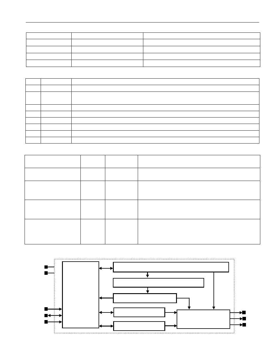
Figure 1. DS1626/DS1726 FUNCTIONAL DIAGRAM
T
COM
T
HIGH
T
LOW
T
H
REGISTER
DIGITAL
COMPARATOR/LOGIC
CONFIGURATION REGISTER AND CONTROL LOGIC
ADDRESS
and
I/O CONTROL
V
DD
CLK/
CNV
SDA
RST
GND
TEMPERATURE SENSOR AND
DS ADC
TEMPERATURE REGISTER
T
L
REGISTER