Rainbow Electronics BA10339FV User Manual
Page 2
INPUT BIAS CURRENT: I
B
(nA)
20
0
20
10
30
40
POWER SUPPLY VOLTAGE: V
–
(V)
40
Ta = 25
°
C
0
60
80
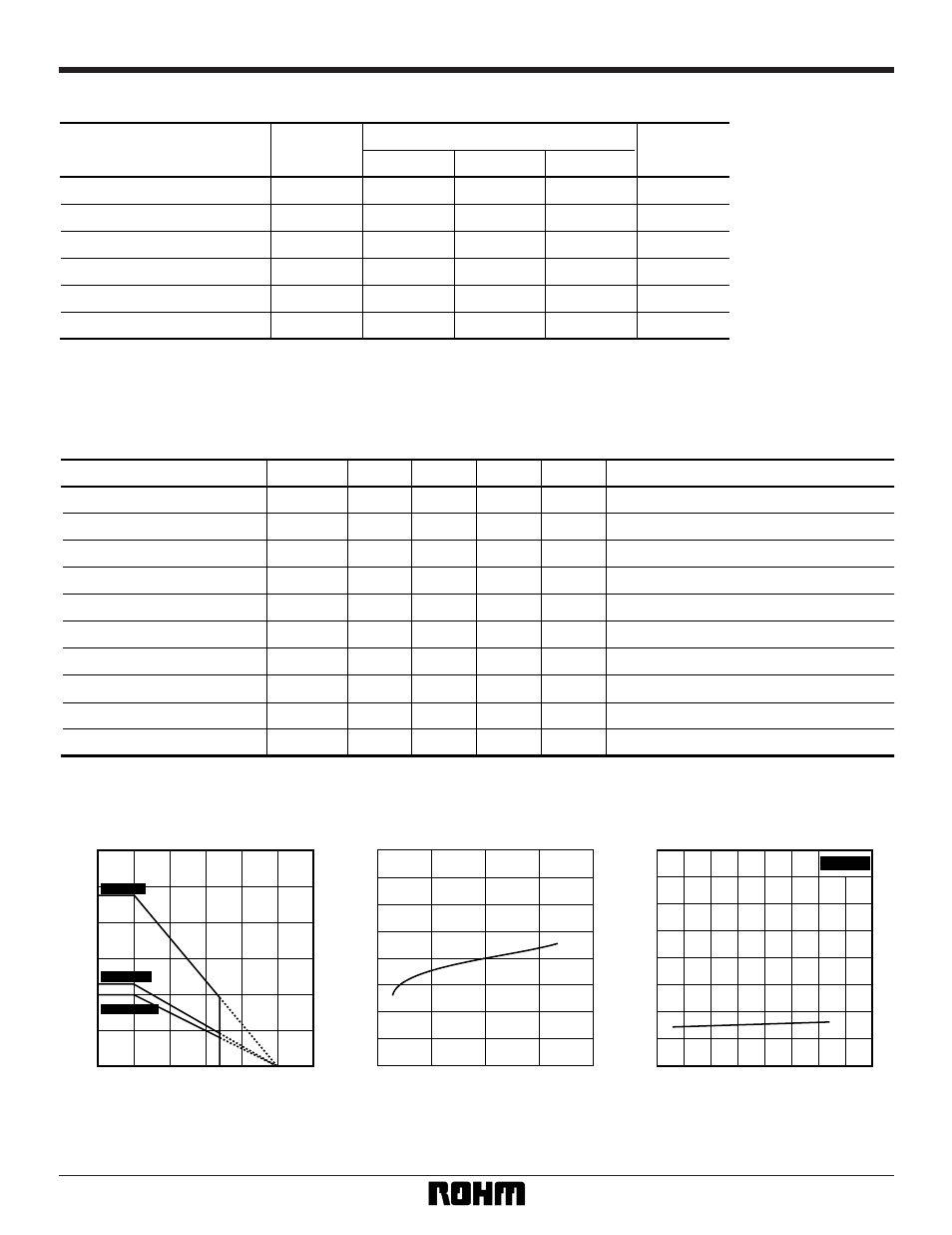
Fig. 3 Input bias current vs. power
supply voltage
2
Standard ICs
BA10339 / BA10339F / BA10339FV
•
Absolute maximum ratings (Ta = 25°C)
Parameter
Symbol
Limits
Unit
BA10339
BA10339F
BA10339FV
V
CC
36 (
±
18)
36 (
±
18)
36 (
±
18)
V
950
∗
450
∗
400
∗
mW
V
ID
±
V
CC
V
V
I
– 0.3 ~ V
CC
V
– 40 ~ + 85
– 40 ~ + 85
– 40 ~ + 85
°
C
– 55 ~ + 125
– 55 ~ + 125
– 55 ~ + 125
°
C
Pd
Topr
Tstg
±
V
CC
– 0.3 ~ V
CC
±
V
CC
– 0.3 ~ V
CC
Power supply voltage
Power dissipation
Differential input voltage
Common-mode input voltage
Operating temperature
Storage temperature
∗
Refer to the Pd characteristic diagram.
∗
The Values for BA10339F and BA10339FV are those when it is mounted on a glass epoxy board (50mm
×
50mm
×
1.6mm).
•
Electrical characteristics (unless otherwise noted, Ta = 25°C, V
CC
= + 5V)
Parameter
Symbol
Min.
Typ.
Max.
Unit
Conditions
V
IO
—
2
5
mV
V
O
= 1.4V
I
IO
—
5
50
nA
I
B
—
25
250
nA
V
O
= 1.4V
V
ICM
0
—
V
CC
– 1.5
V
—
A
V
—
106
—
dB
R
L
= 15k
Ω
I
Q
—
0.8
2
mA
I
sink
6
16
—
mA
V
OL
—
250
400
mV
I
leak
—
0.1
—
nA
t
r
—
1.3
—
µ
s
| I
IN
+
– I
IN
–
| , V
O
= 1.4V
R
L
=
∞
, on All Comparators
R
L
= 5.1k
Ω
, V
RL
= 5V
V
IN
–
= 1V, V
IN
+
= 0V, V
O
= 1.5V
V
IN
–
= 1V, V
IN
+
= 0V, I
sink
= 3mA
V
IN
+
= 1V, V
IN
–
= 0V, V
O
= 5V
Input offset voltage
Input offset current
Input bias current
Common-mode input voltage
Voltage gain
Quiescent current
Output sink current
Output saturation voltage
Output leakage current
Response time
•
Electrical characteristic curves
POWER DISSIPATION: Pd (mW)
AMBIENT TEMPERATURE: Ta (
°
C)
Fig. 1 Power dissipation vs. ambient
temperature
1200
1000
800
600
400
200
0
0
25
50
75 85 100
125
150
BA10339FV
BA10339F
BA10339
QUIESCENT CURRENT: I
Q
(mA)
0
20
10
30
40
POWER SUPPLY VOLTAGE: V
+
(V)
1.2
Ta = 25
°
C
R
L
=
∞
0.6
0.8
1.0
Fig. 2 Quiescent current vs. power
supply voltage