Description, Typical operating circuit – Rainbow Electronics DS12887A User Manual
Page 2
DS12887A
2 of 2
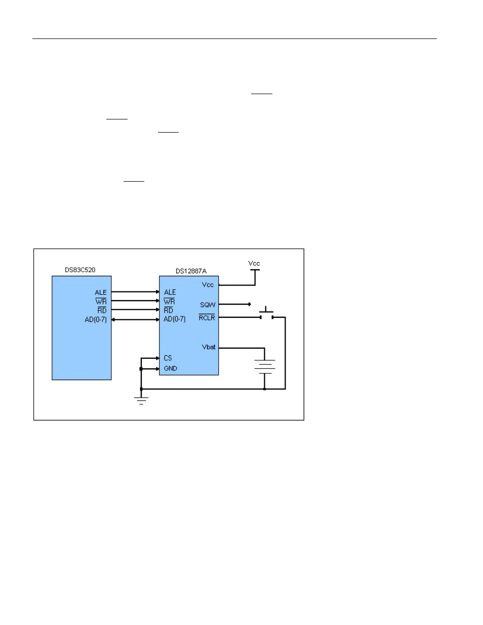
DESCRIPTION
The DS12887A real-time clock plus RAM is designed to be a direct replacement for the DS1287A. The
DS12887A is identical in form, fit, and function to the DS1287A, and includes additional 64 bytes of
general-purpose RAM. Access to this additional RAM space is determined by the logic level presented on
AD6 during the address portion of an access cycle. The
RCLR
pin is used to clear (set to logic 1) all 114
bytes of general-purpose RAM but does not affect the RAM associated with the real-time clock. In order
to clear the RAM,
RCLR
must be forced to an input logic 0 (-0.3V to +0.8V) during battery-backup mode
when V
CC
is not applied. The
RCLR
function is designed to be used by human interface (shorting to
ground manually or by switch) and not to be driven with external buffers.
For a complete description of operating conditions, electrical characteristics, bus timing and pin
descriptions other than
RCLR
, refer to the DS12887 data sheet.
Note: Pins 2, 3, 16, 20, and 22 are missing by design. This device cannot be stored or shipped in conductive material that will give a continuity
path between the RAM clear pin and ground.
TYPICAL OPERATING CIRCUIT