Functional description – Rainbow Electronics ADC08832 User Manual
Page 12

Functional Description
1.0 MULTIPLEXER ADDRESSING
The design of these converters utilizes a comparator struc-
ture with built-in sample-and-hold which provides for a differ-
ential analog input to be converted by a successive approxi-
mation routine.
The actual voltage converted is always the difference be-
tween an assigned “+” input terminal and a “−” input terminal.
The polarity of each input terminal of the pair indicates which
line the converter expects to be the most positive. If the as-
signed “+” input voltage is less than the “−” input voltage the
converter responds with an all zeros output code.
A unique input multiplexing scheme has been utilized to pro-
vide multiple analog channels with software-configurable
single-ended, or differential operation. The analog signal
conditioning required in transducer-based data acquisition
systems is significantly simplified with this type of input flex-
ibility. One converter package can now handle ground refer-
enced inputs, differential inputs, as well as signals with some
arbitrary reference voltage.
A particular input configuration is assigned during the MUX
addressing sequence, prior to the start of a conversion. The
MUX address selects which of the analog inputs are to be
enabled and whether this input is single-ended or differential.
In addition to selecting differential mode the polarity may
also be selected. Channel 0 may be selected as the positive
input and channel 1 as the negative input or vice versa. This
programmability is illustrated by the MUX addressing codes
for the ADC08832.
The MUX address is shifted into the converter via the DI line.
Because the ADC08831 contains only one differential input
channel with a fixed polarity assignment, it does not require
addressing.
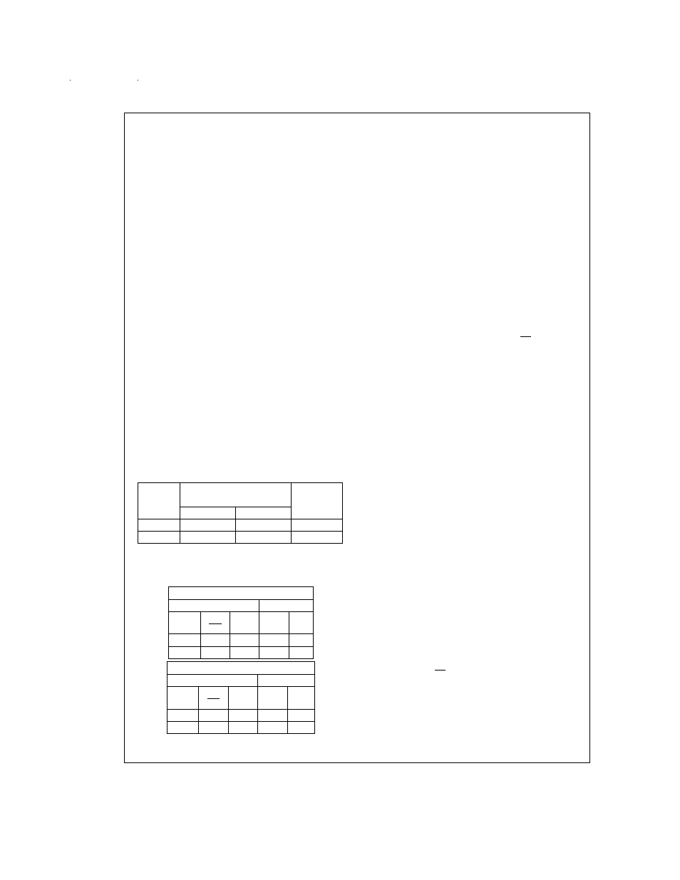
TABLE 1. Multiplexer/Package Options
Part
Number
Number of Analog
Channels
Number of
Package
Pins
Single-Ended
Differential
ADC08831
1
1
8 or 14
ADC08832
2
1
8 or 14
MUX Addressing:
ADC08832
Single-Ended MUX Mode
MUX Address
Channel #
Start
Bit
SGL/
DIF
ODD/
SIGN
0
1
1
1
0
+
1
1
1
+
Differential MUX Mode
MUX Address
Channel #
Start
Bit
SGL/
DIF
ODD/
SIGN
0
1
1
0
0
+
−
1
0
1
−
+
Since the input configuration is under software control, it can
be modified as required before each conversion. A channel
can be treated as a single-ended, ground referenced input
for one conversion; then it can be reconfigured as part of a
differential channel for another conversion.
The analog input voltages for each channel can range from
50mV below ground to 50mV above V
CC
(typically 5V) with-
out degrading conversion accuracy.
2.0 THE DIGITAL INTERFACE
A most important characteristic of these converters is their
serial data link with the controlling processor. Using a serial
communication format offers two very significant system im-
provements. It allows many functions to be included in a
small package and it can eliminate the transmission of low
level analog signals by locating the converter right at the
analog sensor; transmitting highly noise immune digital data
back to the host processor.
To understand the operation of these converters it is best to
refer to the Timing Diagrams and Functional Block Diagram
and to follow a complete conversion sequence. For clarity, a
separate timing diagram is shown for each device.
1.
A conversion is initiated by pulling the CS (chip select)
line low. This line must be held low for the entire conver-
sion. The converter is now waiting for a start bit and its
MUX assignment word, if applicable.
2.
On each rising edge of the clock the status of the data in
(DI) line is clocked into the MUX address shift register.
The start bit is the first logic “1” that appears on this line
(all leading zeros are ignored). Following the start bit the
converter expects the next 2 bits to be the MUX assign-
ment word.
3.
When the start bit has been shifted into the start location
of the MUX register, and the input channel has been as-
signed, a conversion is about to begin. An interval of
1
⁄
2
clock period (where nothing happens) is automatically
inserted to allow the selected MUX channel to settle to a
final analog input value. The DI line is disabled at this
time. It no longer accepts data.
4.
The data out (DO) line now comes out of TRI-STATE
and provides a leading zero for this one clock period of
MUX settling time.
5.
During the conversion the output of the SAR comparator
indicates whether the analog input is greater than (high)
or less than (low) a series of successive voltages gener-
ated internally from a ratioed capacitor array (first 5 bits)
and a resistor ladder (last 3 bits). After each comparison
the comparator’s output is shipped to the DO line on the
falling edge of CLK. This data is the result of the conver-
sion being shifted out (with the MSB first) and can be
read by the processor immediately.
6.
After 8 clock periods the conversion is completed.
7.
The stored data in the successive approximation register
is loaded into an internal shift register. The data, LSB
first, is automatically shifted out the DO line after the
MSB first data stream. The DO line then goes low and
stays low until CS is returned high. The ADC08831 is an
exception in that its data is only output in MSB first for-
mat.
8.
The DI and DO lines can be tied together and controlled
through a bidirectional processor I/O bit with one wire.
This is possible because the DI input is only “looked-at”
during the MUX addressing interval while the DO line is
still in a high impedance state.
www.national.com
12
