Rainbow Electronics MAX5953D User Manual
Page 6
MAX5953A/MAX5953B/MAX5953C/MAX5953D
IEEE 802.3af PD Interface and PWM Controllers
with Integrated Power MOSFETs
6
_______________________________________________________________________________________
ELECTRICAL CHARACTERISTICS (DC-DC Controller) (continued)
(All voltages referenced to GND, unless otherwise noted. V
HVIN
= +48V, C
INBIAS
= 1µF, C
REGOUT
= 2.2µF, R
RTCT
= 25k
Ω, C
RTCT
=
100pF, C
BST
= 0.22µF, V
CSS
= V
CS
= 0V, V
RAMP
= V
DCUVLO
= 3V, T
J
= 0°C to +125°C, unless otherwise noted. Typical values are at
T
J
= +25°C, unless otherwise noted.) (Note 1)
PARAMETER
SYMBOL
CONDITIONS
MIN
TYP
MAX
UNITS
UNDERVOLTAGE LOCKOUT (DCUVLO)
Threshold Voltage
V
REF,DCUVLO
V
DCUVLO
rising
1.14
1.26
1.38
V
Hysteresis
V
HYS,DCUVLO
140
mV
Input Bias Current
I
IN,DCUVLO
V
DCUVLO
= 3V
-100
+100
nA
SUPPLY CURRENT
From V
HVIN
= 11V to 76V,
V
CSS
= 0V, V
INBIAS
= 11V
0.7
1.5
From V
INBIAS
= 11V to 76V,
V
CSS
= 0V, V
HVIN
= 76V
4.4
6.4
Supply Current
From V
HVIN
= 76V, V
OPIO
= 4V
7
mA
Standby Supply Current
V
DCUVLO
= 0V
1
mA
Note 1:
Limits at 0°C are guaranteed by design, unless otherwise noted.
Note 2:
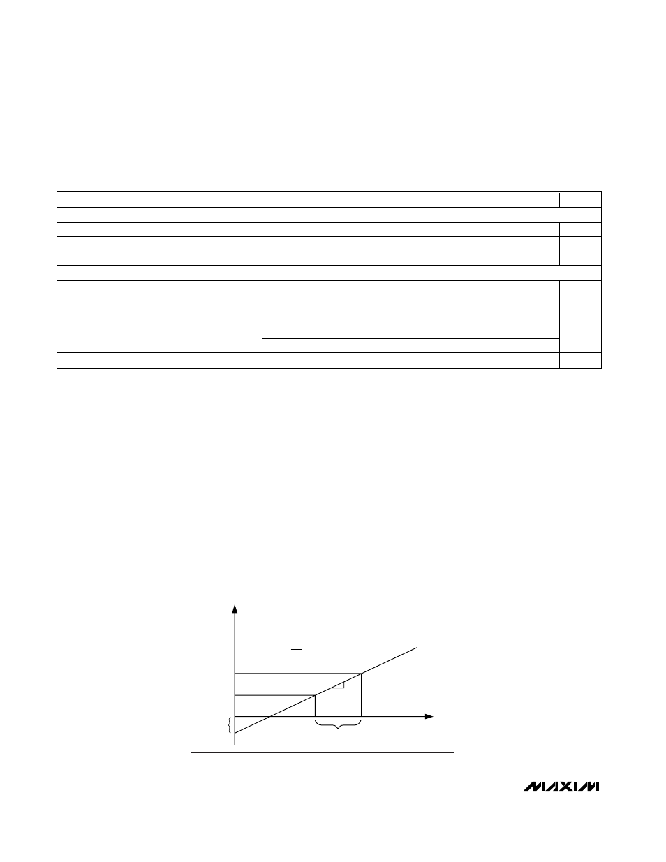
The input offset current is illustrated in Figure 1.
Note 3:
Effective differential input resistance is defined as the differential resistance between V+ and V
EE
without any external
resistance.
Note 4:
Classification current is turned off whenever the IC is in power mode.
Note 5:
See Table 2 in the Classification Mode section. R
DISC
and R
RCLASS
must be 1%, 100ppm or better. I
CLASS
includes the IC
bias current and the current drawn by R
DISC
.
Note 6:
See the Thermal Dissipation section.
Note 7:
When UVLO is connected to the midpoint of an external resistor-divider with a series resistance of 25.5k
Ω (±1%), the turn-
on threshold set point for the power mode is defined by the external resistor-divider. Make sure the voltage on UVLO does
not exceed its maximum rating of 8V when V
IN
is at the maximum voltage.
Note 8:
When V
UVLO
is below V
TH,G,UVLO
, the MAX5953A/MAX5953C set the turn-on voltage threshold internally (V
UVLO,ON
).
Note 9:
An input voltage or V
UVLO
glitch below their respective thresholds shorter than or equal to t
OFF_DLY
does not cause the
MAX5953A/MAX5953B/MAX5953C/MAX5953D to exit power-on mode (as long as the input voltage remains above an
operable voltage level of 12V).
Note 10: Guaranteed by design, not tested in production for MAX5953B/MAX5953D.
Note 11: PGOOD references to OUT while PGOOD references to V
EE
.
Note 12: Output switching frequency is
1
/
2
oscillator frequency.
Figure 1. Effective Differential Input Resistance/Offset Current
I
IN
I
INi + 1
I
INi
I
OFFSET
dR
i
1V
V
INi
V
INi + 1
I
OFFSET
≅ I
INi
-
V
INi
dR
i
dR
i
≅
(V
INi + 1
- V
INi
)
=
1V
(I
INi + 1
- I
INi
)
(I
INi + 1
- I
INi
)
V
IN