Rainbow Electronics MAX5382 User Manual
Page 9
MAX5380/MAX5381/MAX5382
Low-Cost, Low-Power, 8-Bit DACs with
2-Wire Serial Interface in SOT23
_______________________________________________________________________________________
9
Power-On Reset
The MAX5380/MAX5381/MAX5382 have a power-on
reset circuit to set the DAC’s output to 0 when V
DD
is
first applied or when V
DD
dips below 1.7V (typ). This
ensures that unwanted DAC output voltages will not
occur immediately following a system startup, such as
after a loss of power. The output glitch at startup is typi-
cally less than 50mV.
Shutdown Mode
The MAX5380/MAX5381/MAX5382 include a software-
controlled shutdown mode that reduces the supply cur-
rent to <1µA. All internal circuitry is disabled, and an
internal 10k
Ω resistor is placed from OUT to GND to
ensure 0V at OUT while in shutdown. The device enters
shutdown in less than 5µs and exits shutdown in less
than 50µs.
Digital Section
Serial Interface
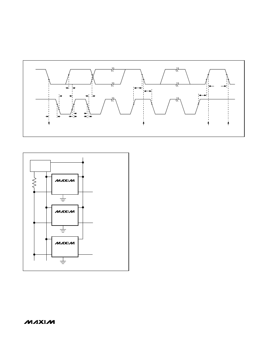
The MAX5380/MAX5381/MAX5382 use a simple 2-wire
serial interface requiring only two I/O lines (2-wire bus)
of a standard microprocessor (µP) port. Figure 3 shows
the timing diagram for signals on the 2-wire bus.
The two bus lines (SDA and SCL) must be high when
the bus is not in use. The MAX5380/MAX5381/
MAX5382 are receive-only devices (slaves) and must
be controlled by a bus master device. Figure 4 shows a
typical application where up to four devices can be
connected to the bus, provided they have different
address settings. External pull-up resistors are not nec-
essary on these lines (when driven by push-pull dri-
vers), though these DACs can be used in applications
where pull-up resistors are required (such as in I
2
C
systems) to maintain compatibility with existing circuit-
ry. The serial interface operates at SCL rates up to
400kHz. The SDA state is allowed to change only while
SCL is low, with the exception of START and STOP con-
ditions as shown in Figure 5. Each transmission con-
sists of a START condition sent by the bus master
SCL
SDA
t
LOW
t
HIGH
t
F
t
R
t
HD:
STA
t
HD:
DAT
t
HD:
STA
t
SU:
DAT
t
SU:
STA
t
BUF
t
SU:
STO
START CONDITION
STOP CONDITION
REPEATED START CONDITION
START CONDITION
Figure 3. 2-Wire Serial Interface Timing Diagram
µC
SDA
SCL
R
S
*
V
DD
OFFSET ADJUSTMENT
THRESHOLD ADJUSTMENT
GAIN ADJUSTMENT
*R
S
IS OPTIONAL.
SCL
SDA
V
DD
OUT
MAX5380M
2V REFERENCE
SCL
SDA
V
DD
OUT
MAX5381N
4V REFERENCE
SCL
SDA
V
DD
OUT
MAX5382P
V
DD
REFERENCE
Figure 4. Typical Application Circuit