Detailed description, Table 1. unipolar code output voltage – Rainbow Electronics MAX5382 User Manual
Page 8
MAX5380/MAX5381/MAX5382
Low-Cost, Low-Power, 8-Bit DACs with
2-Wire Serial Interface in SOT23
8
_______________________________________________________________________________________
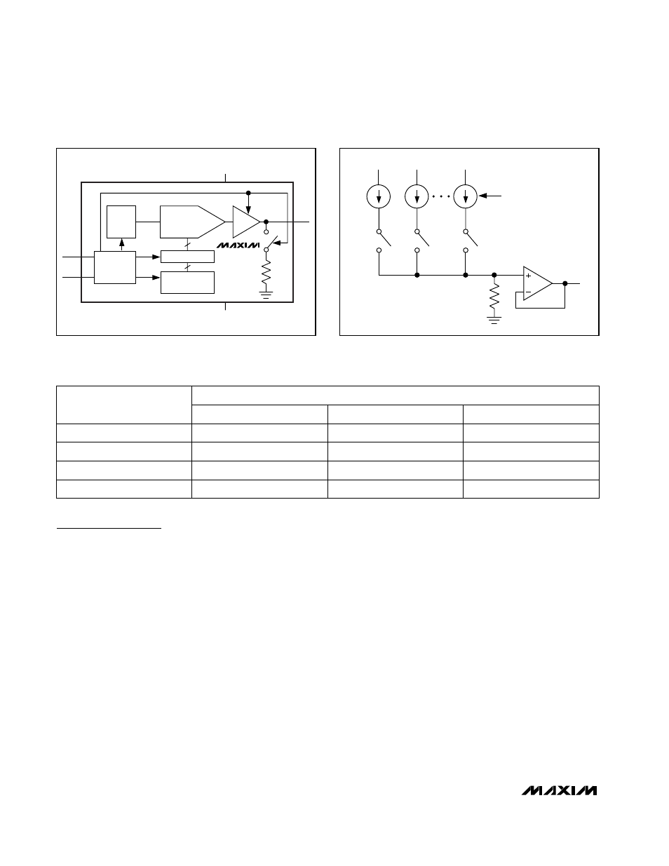
Detailed Description
The MAX5380/MAX5381/MAX5382 voltage-output, 8-bit
digital-to-analog converters (DACs) offer full 8-bit perfor-
mance with less than 1LSB integral nonlinearity error
and less than 1LSB differential nonlinearity error, ensur-
ing monotonic performance. The devices use a simple
2-wire, fast-mode I
2
C-compatible serial interface that
operates at up to 400kHz. The MAX5380/MAX5381/
MAX5382 include an internal reference, an output
buffer, and a low-current shutdown mode, which make
these devices ideal for low-power, highly integrated
applications (See Figure 1. Functional Diagram).
Analog Section
The MAX5380/MAX5381/MAX5382 employ a current-
steering DAC topology as shown in Figure 2. At the core
of the DAC is a reference voltage-to-current converter
(V/I) that generates a reference current. This current is
mirrored to 255 equally weighted current sources. DAC
switches control the outputs of these current mirrors so
that only the desired fraction of the total current-mirror
currents is steered to the DAC output. The current is
then converted to a voltage across a resistor, and this
voltage is buffered by the output buffer amplifier.
Output Voltage
Table 1 shows the relationship between the DAC code
and the analog output voltage. The 8-bit DAC code is
binary unipolar with 1LSB = V
REF
/ 256. The MAX5380/
MAX5381 have a full-scale output voltage of (+2V -
1LSB) and (+4V - 1LSB), respectively, set by the internal
references. The MAX5382 has a full-scale output volt-
age of (0.9
x
V
DD
- 1LSB).
Output Buffer
The DAC voltage output is an internally buffered unity-
gain follower that typically slews at ±0.4V/µs. The out-
put can swing from 0 to full scale. With a 1/4 FS to 3/4
FS output transition, the amplifier outputs typically settle
to 1/2LSB in less than 5µs when loaded with 10k
Ω in
parallel with 50pF. The buffer amplifiers are stable with
any combination of resistive loads >10k
Ω and capaci-
tive loads <50pF.
V
REF
SW1
SW2
SW255
OUT
Figure 2. Current-Steering Topology
V
DD
OUT
10k
GND
SDA
SCL
255
8
CURRENT-
STEERING
DAC
DATA LATCH
SERIAL INPUT
REGISTER
CONTROL
LOGIC
MAX5380
MAX5381
MAX5382
REF
Figure 1. Functional Diagram
Table 1. Unipolar Code Output Voltage
0000 0001
0.9 x V
DD
/ 256
15.6mV
7.8mV
0000 0000
0
0
0
1000 0000
0.9 x V
DD
/ 2
+2V
+1V
1111 1111
0.9 x V
DD
x (255 / 256)
4V x (255 / 256)
2V x (255 / 256)
MAX5382
MAX5381
MAX5380
DAC CODE
OUTPUT VOLTAGE