Detailed description, Pin description – Rainbow Electronics MAX5101 User Manual
Page 6
MAX5101
+2.7V to +5.5V, Low-Power, Triple, Parallel
8-Bit DAC with Rail-to-Rail Voltage Outputs
6
_______________________________________________________________________________________
Detailed Description
Digital-to-Analog Section
The MAX5101 uses a matrix decoding architecture for the
digital-to-analog converters (DACs). The internal refer-
ence voltage is connected to V
DD
and divided down by a
resistor string placed in a matrix fashion. Row and col-
umn decoders select the appropriate tab from the resistor
string to provide the needed analog voltages. The resistor
network converts the 8-bit digital input into an equivalent
analog output voltage in proportion to the supply voltage
(V
DD
). The resistor string presents a code-independent
input impedance to the supply and guarantees a monoto-
nic output.
The voltages are buffered by rail-to-rail op amps con-
nected in a follower configuration to provide a rail-to-rail
output (see Functional Diagram).
Output Buffer Amplifiers
The DAC outputs are internally buffered by a precision
amplifier with a typical slew rate of 0.6V/µs. The typical
settling time to ±1/2LSB at the output is 6µs when
loaded with 10k
Ω in parallel with 100pF.
DAC Reference Voltage
The MAX5101’s reference is internally tied to V
DD
. The
output voltage (V
OUT
) for any DAC is represented by a
digitally programmable voltage source as follows:
V
OUT
= (N
B
· V
DD
) / 256
where N
B
is the numeric value of the DAC binary input
code.
Digital Inputs and Interface Logic
In the MAX5101, address lines A0 and A1 select the DAC
that receives data from D0–D7, as shown in Table 1.
When WR is low, the addressed DAC’s input latch is
transparent. Data is latched when WR is high. The DAC
outputs (OUTA, OUTB) represent the data held in the
three 8-bit input latches. To avoid output glitches in the
MAX5101, ensure that data is valid before WR goes low.
Low-Power Shutdown Mode
The MAX5101 features a software shutdown mode. A
write performed to address A1 = H and A0 = H causes
the device to shut down. A subsequent write to any of
the other three addresses disables shutdown and turns
the analog circuitry on. As the MAX5101 comes out of
shutdown, all registers retain their digital values prior to
shutdown. However, when the device powers up (i.e.,
V
DD
ramps up), all latches are internally preset with
code 00 hex. In shutdown, the output amplifiers enter a
high-impedance state. When bringing the device out of
shutdown, allow 13µs for the output to stabilize.
Power-Supply Bypassing and
Ground Management
Digital or AC transient signals on GND can create noise
at the analog output. Return GND to the highest-quality
ground available. Bypass V
DD
with a 0.1µF capacitor,
located as close to V
DD
and GND as possible.
Careful PC board ground layout minimizes crosstalk
between the DAC outputs and digital inputs.
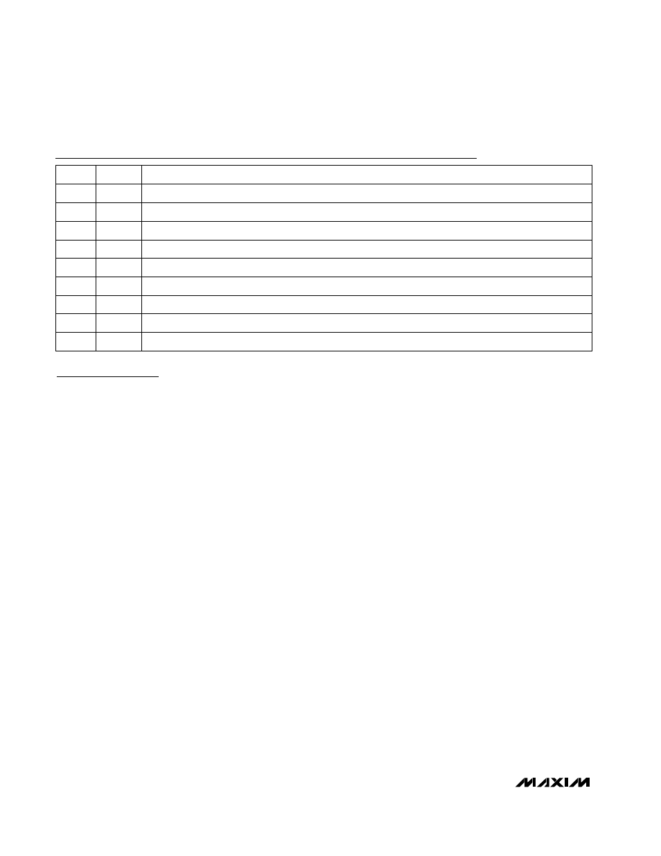
NAME
FUNCTION
1
OUTB
DAC B Voltage Output
2
OUTA
DAC A Voltage Output
PIN
3
V
DD
Positive Supply Voltage. Bypass V
DD
to GND using a 0.1µF capacitor.
4
WR
Write Input (active low). Use WR to load data into the DAC input latch selected by A0 and A1.
15
GND
Ground
14
A0
DAC Address Select Bit (LSB)
13
A1
DAC Address Select Bit (MSB)
5–12
D7–D0
Data Inputs 7–0
16
OUTC
DAC C Voltage Output
Pin Description