Rainbow Electronics MAX5101 User Manual
General description, Applications, Features
For free samples & the latest literature: http://www.maxim-ic.com, or phone 1-800-998-8800.
For small orders, phone 1-800-835-8769.
General Description
The MAX5101 parallel-input, voltage-output, triple 8-bit
digital-to-analog converter (DAC) operates from a sin-
gle +2.7V to +5.5V supply and comes in a space-sav-
ing 16-pin TSSOP package. Internal precision buffers
swing Rail-to-Rail
®
. For all three DACs, the internal ref-
erence voltage is tied to V
DD
.
The MAX5101 has separate input latches for each of its
three DACs. Data is transferred to the input latches
from a common 8-bit input port. The DACs are individu-
ally selected through address inputs A0 and A1 and
are updated by bringing WR low.
The MAX5101 features a 1µA software shutdown mode,
as well as a power-on reset mode that resets all regis-
ters to code 00 hex on power-up.
Applications
Digital Gain and Offset Adjustment
Programmable Attenuators
Portable Instruments
Power-Amp Bias Control
Features
♦ +2.7V to +5.5V Single-Supply Operation
♦ Ultra-Low Supply Current
0.3mA while Operating
1µA in Software Shutdown Mode
♦ Ultra-Small 16-Pin TSSOP Package
♦ Output Buffer Amplifiers Swing Rail-to-Rail
♦ Power-On Reset Sets All Registers to Zero
MAX5101
+2.7V to +5.5V, Low-Power, Triple, Parallel
8-Bit DAC with Rail-to-Rail Voltage Outputs
________________________________________________________________ Maxim Integrated Products
1
16
15
14
13
12
11
10
9
1
2
3
4
5
6
7
8
OUTB
OUTC
GND
A0
A1
D0
D1
D2
D3
TOP VIEW
MAX5101
TSSOP
OUTA
V
DD
D6
WR
D7
D5
D4
19-1560; Rev 0; 10/99
PART
MAX5101AEUE
MAX5101BEUE
-40°C to +85°C
-40°C to +85°C
TEMP. RANGE
PIN-
PACKAGE
16 TSSOP
16 TSSOP
Pin Configuration
Ordering Information
INL
(LSB)
±1
±2
Rail-to-Rail is a registered trademark of Nippon Motorola, Ltd.
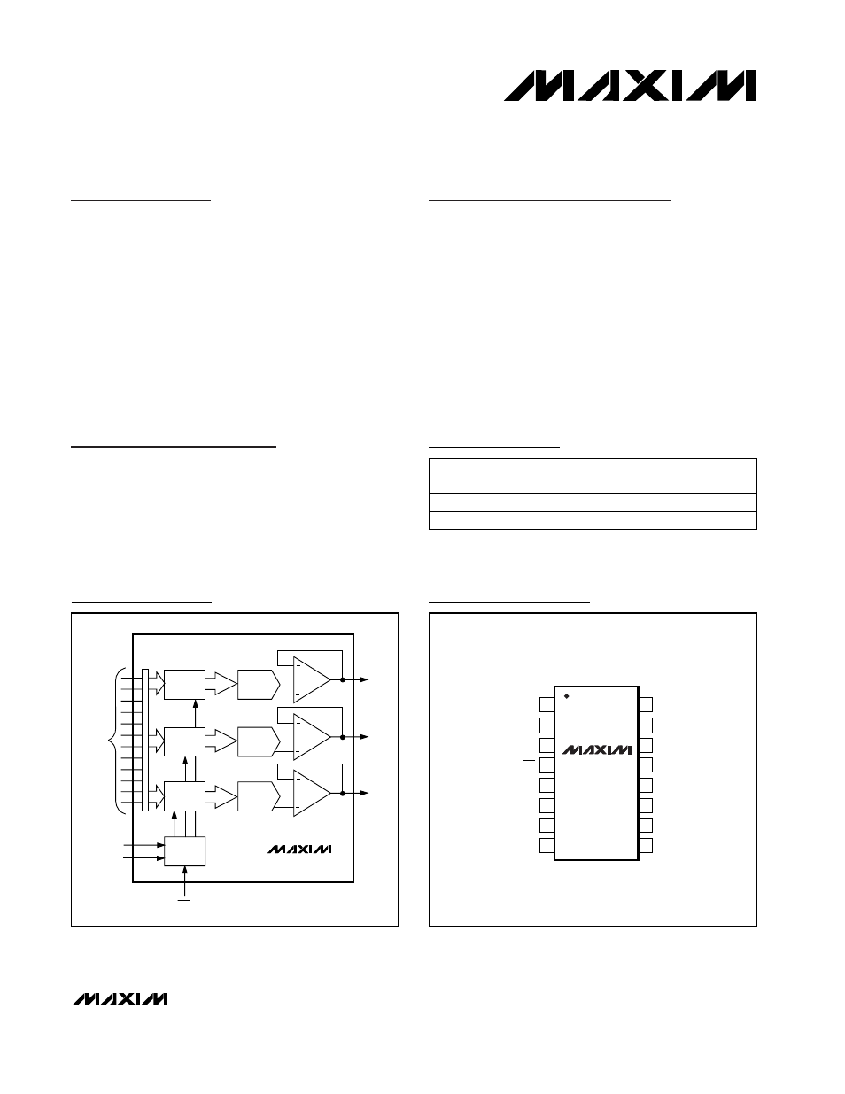
Functional Diagram
OUTB
OUTC
DAC B
DAC C
INPUT
LATCH B
CONTROL
LOGIC
A0
D0–D7
WR
OUTA
DAC A
INPUT
LATCH A
A1
INPUT
LATCH C
MAX5101