Preliminary w78c52d, Block diagram, Xtal1 – Rainbow Electronics W78C52D User Manual
Page 4: Xtal2, 4 - psen program store enable output, active low, Psen
Preliminary W78C52D
- 4 -
PSEN
Program Store Enable Output, active low.
PSEN
enables the external ROM onto the Port 0
address/data bus during fetch and MOVC operations.
PSEN
goes to a high impedance state during
reset with a weak pull-up.
XTAL1
Crystal 1. This is the crystal oscillator input. This pin may be driven by an external clock.
XTAL2
Crystal 2. This is the crystal oscillator output. It is the inversion of XTAL1.
V
SS
, V
DD
Power Supplies. These are the chip ground and positive supplies.
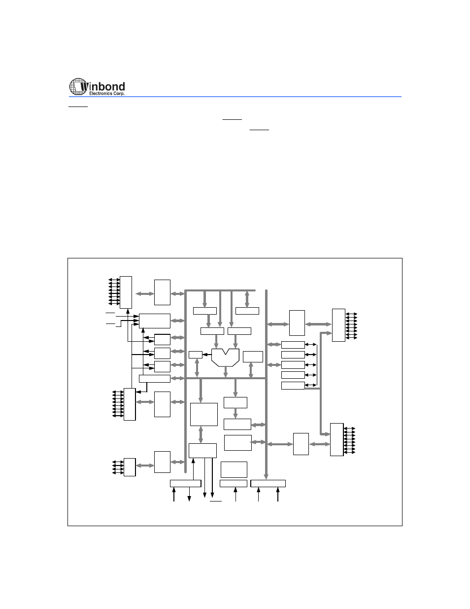
BLOCK DIAGRAM
P3.0
~
P3.7
P1.0
~
P1.7
ALU
Port 0
Latch
Port 1
Latch
Timer
1
Timer
0
Timer
2
Port
1
UART
XTAL1
PSEN
ALE
GND
VDD
RST
XTAL2
Oscillator
Interrupt
PSW
Instruction
Decoder
&
Sequencer
Reset Block
Bus & Clock
Controller
SFR RAM
Address
Power control
256 bytes
RAM & SFR
Stack
Pointer
B
Addr. Reg.
Incrementor
PC
DPTR
Temp Reg.
T2
T1
ACC
Port 3
Latch
Port 4
Latch
Port
3
Port 2
Latch
P4.0
~
P4.3
Port
4
Port
0
Port
2
P2.0
~
P2.7
P0.0
~
P0.7
INT2
INT3
Watchdog
Timer
8K bytes
ROM