Reset – Rainbow Electronics MAX7502 User Manual
Page 10

MAX7500/MAX7501/MAX7502
Shutdown
Set bit D0 in the configuration register to 1 to place the
MAX7500/MAX7501/MAX7502 in shutdown mode and
reduce supply current to 3µA.
Power-Up and Power-Down
The MAX7500/MAX7501/MAX7502 power up to a
known state, as indicated in
Table
2. Some of these
settings are summarized below:
• Comparator mode
• T
OS
= +80
°C
• T
HYST
= +75
°C
• OS active low
• Pointer = 00
Internal Registers
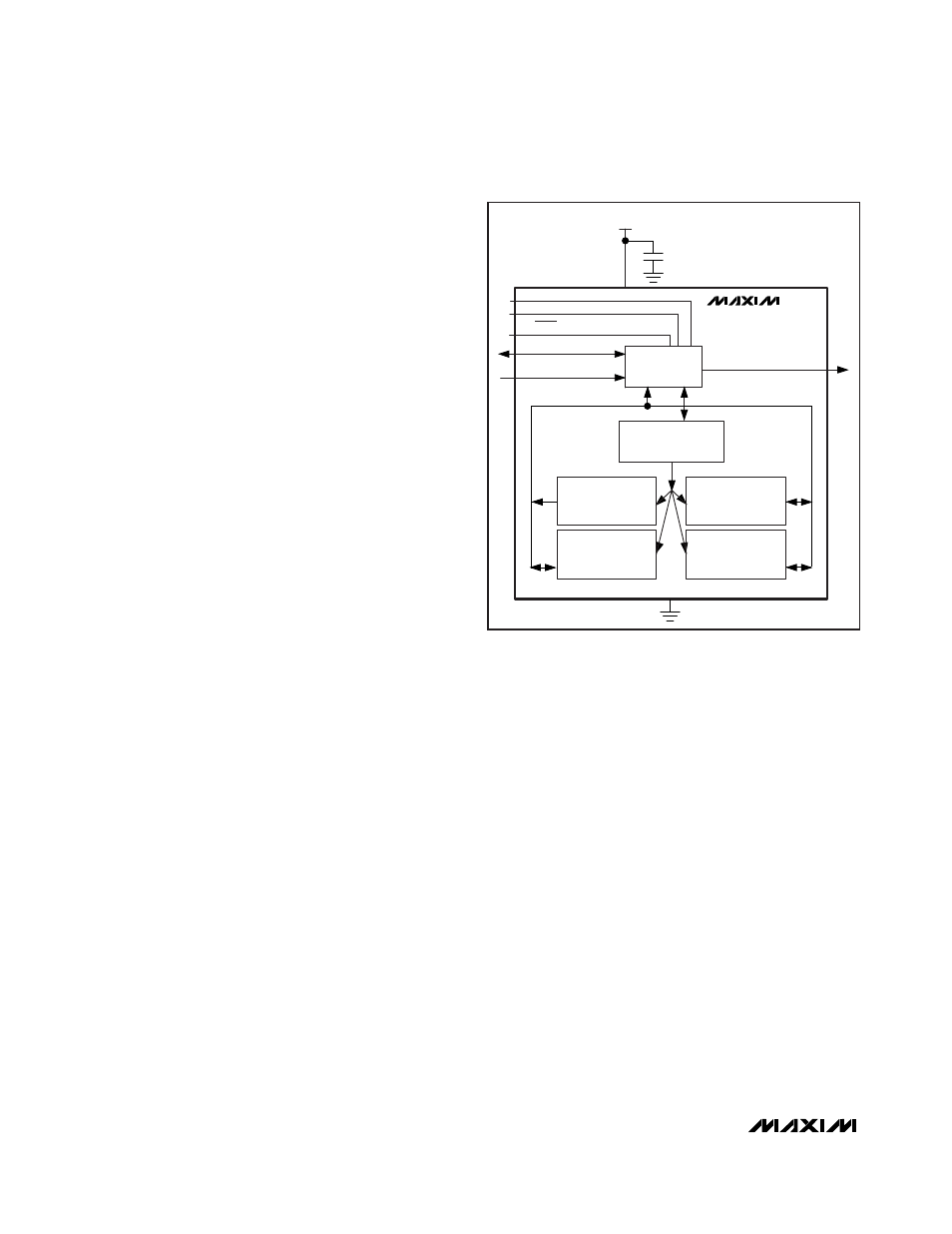
The MAX7500/MAX7501/MAX7502s’ pointer register
selects between four data registers. See
Figure
5. At
power-up, the pointer is set to read the temperature
register at address 00. The pointer register latches the
last location to which it was set. All registers are read
and write, except the temperature register, which is
read only.
Write to the configuration register by writing an address
byte, a data pointer byte, and a data byte. If 2 data
bytes are written, the second data byte overrides the
first. If more than 2 data bytes are written, only the first
2 bytes are recognized while the remaining bytes are
ignored. The T
OS
and T
HYST
registers require 1
address byte and 1 pointer byte and 2 data bytes. If
only 1 data byte is written, it is saved in bits D15–D8 of
the respective register. If more than 2 data bytes are
written, only the first 2 bytes are recognized while the
remaining bytes are ignored.
Read from the MAX7500/MAX7501/MAX7502 in one of
two ways. If the location latched in the pointer register
is set from the previous read, the new read consists of
an address byte, followed by retrieving the correspond-
ing number of data bytes. If the pointer register needs
to be set to a new address, perform a read operation
by writing an address byte, pointer byte, repeat start,
and another address byte.
An inadvertent 8-bit read from a 16-bit register, with the
D7 bit low, can cause the MAX7500/MAX7501/
MAX7502 to stop in a state where the SDA line is held
low. Ordinarily, this would prevent any further bus com-
munication until the master sends nine additional clock
cycles or SDA goes high. At that time, a stop condition
resets the device. With the MAX7500/MAX7501/
MAX7502, if the additional clock cycles are not gener-
ated by the master, the bus resets and unlocks after
the bus timeout period has elapsed.
The MAX7501/MAX7502 can be reset by pulsing
RESET low.
Bus Timeout
Communication errors sometimes occur due to noise
pickup on the bus. In the worst case, such errors can
cause the slave device to hold the data line low, there-
by preventing other devices from communicating over
the bus. The MAX7500/MAX7501/MAX7502s’ internal
bus timeout circuit resets the bus and releases the data
line if the line is low for more than 250ms. When the bus
timeout is active, the minimum serial clock frequency is
limited to 6Hz.
RESET
The RESET input on the MAX7501/MAX7502 provides a
way to reset the I
2
C bus and all the internal registers to
their initial POR values. To reset, apply a low pulse with
a duration of at least 1µs to the RESET input.
Digital Temperature Sensors and Thermal
Watchdog with Bus Lockup Protection
10
______________________________________________________________________________________
MAX7500
MAX7501
MAX7502
+V
S
A2/RESET
A1
A0
SDA
SCL
OS
SMBus
INTERFACE
BLOCK
POINTER REGISTER
(SELECTS REGISTER
FOR COMMUNICATION)
DATA
ADDRESS
REGISTER SELECT
GND
TEMPERATURE
(READ ONLY)
POINTER = 0000 0000
T
OS
SET POINT
(READ/WRITE)
POINTER = 0000 0011
T
HYST
SET POINT
(READ/WRITE)
POINTER = 0000 0010
CONFIGURATION
(READ/WRITE)
POINTER = 0000 0001
Figure 5. Block Diagram
