Electrical characteristics – mxl1116 – Rainbow Electronics MXL1116 User Manual
Page 3
MXL1016/MXL1116
Ultra-Fast Precision TTL Comparators
_________________________________________________________________________________________________
3
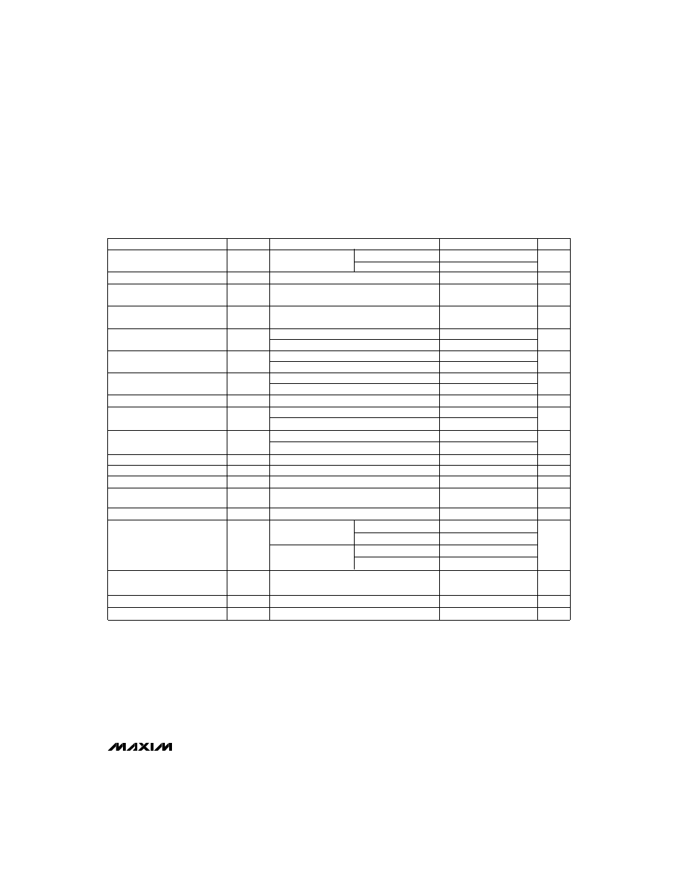
ELECTRICAL CHARACTERISTICS – MXL1116
(V+ = 5V, V– = –5V, V
OUT
(Q) = 1.4V, V
LE
= 0V, T
A
= T
MIN
to T
MAX
, unless otherwise noted. Specifications for V
OS
, I
B
, CMRR and A
V
are valid for single-supply operation, V+ = 5V, V– = 0V.)
PARAMETER
MIN
CONDITIONS
UNITS
Power-Supply Rejection Ratio
TYP
Positive Supply: 4.6V
≤
V+
≤
5.4V
dB
Small-Signal Voltage Gain
MAX
1V
≤
V
OUT
≤
2V, T
A
= +25°C
V/V
Output High Voltage
V
I
SOURCE
= 1mA
60
I
SOURCE
= 10mA
2.4
Positive Supply Current
75
mA
1400
3000
2.7
3.4
Input Offset Voltage
(Note 1)
R
S
≤
100
Ω
mV
3.0
Input Offset-Voltage Drift
0.5
µV/°C
27
2
38
Input Offset Current
(Note 1)
µA
Negative Supply Current
mA
Latch Pin High Input Voltage
1.0
V
Latch Pin Low Input Voltage
±3
V
10
20
Input Bias Current, Sourcing
(Note 2)
5
Latch Input Current
V
LE
= 0V
µA
∆
V
IN
= 100mV,
OD = 5mV
Propagation Delay
(Note 3)
ns
Differential Propagation Delay
(Note 3)
∆
V
IN
= 100mV, OD = 5mV, T
A
= +25°C
ns
Latch Setup Time (Note 4)
ns
5
7
2.0
0.8
–20
–500
12
16
10
14
3
2
Single 5V supply
V–
(V+ – 2.5)
75
90
SYMBOL
PSRR
A
V
V
OH
0
2.5
Negative Supply: –7V
≤
V–
≤
–2V
Input Voltage Range
V
Common-Mode Rejection Ratio
I+
–5V
≤
V
CM
≤
2.5V
dB
V
OS
∆
V
OS
/
∆
T
I
OS
I–
V
IH
V
IL
I
IL
t
PD
∆
t
PD
t
SU
V
CM
CMRR
3.5
µA
I
B
80
100
18
∆
V
IN
= 100mV,
OD = 20mV
Output Low Voltage
V
I
SINK
= 4mA
I
SINK
= 10mA, T
A
= +25°C
0.3
0.5
0.4
V
OL
0V
≤
V
CM
≤
2.5V, V
S
= +5V, 0V
65
90
16
Latch Hold Time (Note 4)
ns
2
t
H
Note 1:
Input offset voltage is defined as the average of the two input offset voltages, measured by forcing first one output, then the
other to 1.4V. Input offset current is defined in the same way.
Note 2:
Input bias current (I
B
) is defined as the average of the two input currents.
Note 3:
t
PD
and
∆
t
PD
cannot be measured in automatic handling equipment with low values of overdrive. Correlation tests have
shown that t
PD
and
∆
t
PD
limits shown can be guaranteed by design, if additional DC tests are performed to guarantee that
all internal bias conditions are correct. For low overdrive conditions, V
OS
is added to overdrive.
Note 4:
Input latch setup time, t
SU
, is the interval in which the input signal must be stable prior to asserting the latch signal. The hold
time, t
H
, is the interval after the latch is asserted in which the input signal must be stable.
T
A
= +25°C
T
A
= +25°C
T
A
= +25°C