Functional description – Rainbow Electronics ADC1001 User Manual
Page 6
Functional Description
The ADC1001 uses an advanced potentiometric resistive
ladder network The analog inputs as well as the taps of
this ladder network are switched into a weighted capacitor
array The output of this capacitor array is the input to a
sampled data comparator This comparator allows the suc-
cessive approximation logic to match the analog difference
input voltage V
IN
(a)bV
IN
(b) to taps on the R network
The most significant bit is tested first and after 10 compari-
sons (80 clock cycles) a digital 10-bit binary code (all
‘‘1’’sefull-scale) is transferred to an output latch and then
an interrupt is asserted (INTR makes a high-to-low tran-
sition) The device may be operated in the free-running
mode by connecting INTR to the WR inut with CSe0 To
ensure start-up under all possible conditions an external
WR pulse is required during the first power-up cycle A con-
version in process can be interrupted by issuing a second
start command
On the high-to-low transition of the WR input the internal
SAR latches and the shift register stages are reset As long
as the CS input and WR input remain low the A D will re-
main in a reset state
Conversion will start from 1 to 8 clock
periods after at least one of these inputs makes a low-to-
high transition
A functional diagram of the A D converter is shown in
Fig-
ure 1
All of the inputs and outputs are shown and the major
logic control paths are drawn in heavier weight lines
The conversion is initialized by taking CS and WR simulta-
neously low This sets the start flip-flop (F F) and the result-
ing ‘‘1’’ level resets the 8-bit shift register resets the Inter-
rupt (INTR) F F and inputs a ‘‘1’’ to the D flop F F1 which
is at the input end of the 10-bit shift register Internal clock
signals then transfer this ‘‘1’’ to the Q output of F F1 The
AND gate G1 combines this ‘‘1’’ output with a clock signal
to provide a reset signal to the start F F If the set signal is
no longer present (either WR or CS is a ‘‘1’’) the start F F is
reset and the 10-bit shift register then can have the ‘‘1’’
clocked in which allows the conversion process to contin-
ue If the set signal were to still be present this reset pulse
would have no effect and the 10-bit shift register would con-
tinue to be held in the reset mode This logic therefore al-
lows for wide CS and WR signals and the converter will start
after at least one of these signals returns high and the inter-
nal clocks again provide a reset signal for the start F F
After the ‘‘1’’ is clocked through the 10-bit shift register
(which completes the SAR search) it causes the new digital
word to transfer to the TRI-STATE output latches When
this XFER signal makes a high-to-low transition the one
shot fires setting the INTR F F An inverting buffer then
supplies the INTR output signal
Note that this SET control of the INTR F F remains low for
aproximately 400 ns If the data output is continuously en-
abled (CS and RD both held low) the INTR output will still
signal the end of the conversion (by a high-to-low tran-
sition) because the SET input can control the Q output of
the INTR F F even though the RESET input is constantly at
a ‘‘1’’ level This INTR output will therefore stay low for the
duration of the SET signal
When data is to be read the combination of both CS and
RD being low will cause the INTR F F to be reset and the
TRI-STATE output latches will be enabled
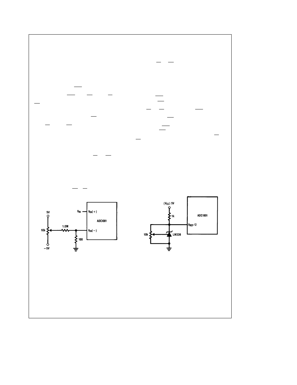
Zero and Full-Scale Adjustment
Zero error can be adjusted as shown in
Figure 2
V
IN
(a) is
forced to a2 5 mV (a
LSB) and the potentiometer is
adjusted until the digital output code changes from 00 0000
0000 to 00 0000 0001
Full-scale is adjusted as shown in
Figure 3
with the V
REF
2
input With V
IN
(a) forced to the desired full-scale voltage
less 1
LSBs (V
FS
b
1
LSBs) V
REF
2 is adjusted until
the digital output code changes from 11 1111 1110 to 11
1111 1111
TL H 5675 – 9
NOTE V
IN
(
b
) should be biased so
that V
IN
(
b
)
t b
0 05V when potentiometer
wiper is set at most negative
voltage position
FIGURE 2 Zero Adjust Circuit
TL H 5675 – 10
FIGURE 3 Full-Scale Adjust
6