Rainbow Electronics ADC1001 User Manual
General description, Features, Key specifications
TL H 5675
ADC1001
10-Bit
m
P
Compatible
AD
Converter
December 1994
ADC1001 10-Bit mP Compatible A D Converter
General Description
The ADC1001 is a CMOS 10-bit successive approximation
A D converter The 20-pin ADC1001 is pin compatible with
the ADC0801 8-bit A D family The 10-bit data word is read
in two 8-bit bytes formatted left justified and high byte first
The six least significant bits of the second byte are set to
zero as is proper for a 16-bit word
Differential inputs provide low frequency input common
mode rejection and allow offsetting the analog range of the
converter In addition the reference input can be adjusted
enabling the conversion of reduced analog ranges with 10-
bit resolution
Features
Y
ADC1001 is pin compatible with ADC0801 series 8-bit
A D converters
Y
Compatible with NSC800 and 8080 mP derivatives
no
interfacing logic needed
Y
Easily interfaced to 6800 mP derivatives with minimal
external logic
Y
Differential analog voltage inputs
Y
Logic inputs and outputs meet both MOS and TTL volt-
age level specifications
Y
Works with 2 5V (LM336) voltage reference
Y
On-chip clock generator
Y
0V to 5V analog input voltage range with single 5V sup-
ply
Y
Operates ratiometrically or with 5 V
DC
2 5 V
DC
or ana-
log span adjusted voltage reference
Y
0 3
standard width 20-pin DIP package
Key Specifications
Y
Resolution
10 bits
Y
Linearity error
g
1 LSB
Y
Conversion time
200mS
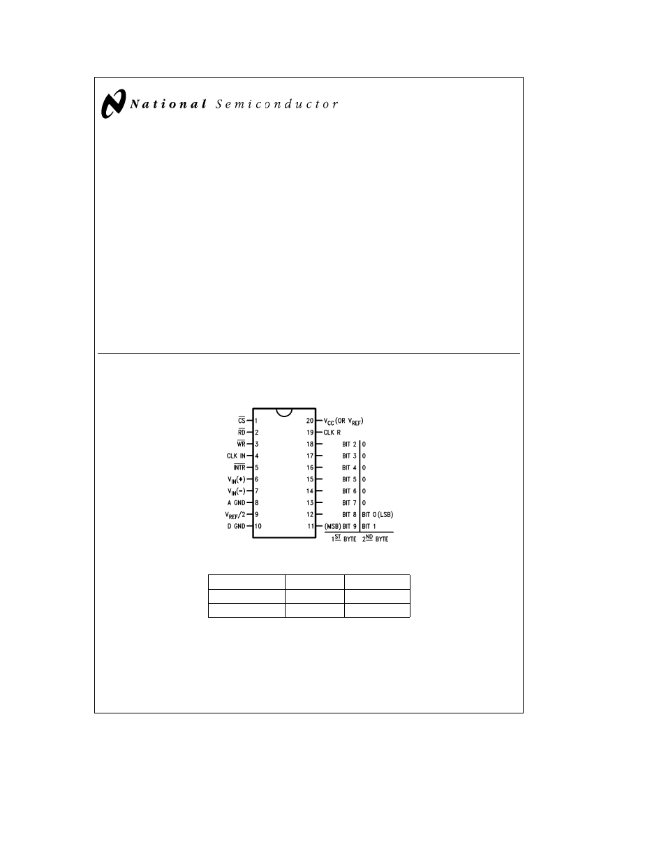
Connection Diagram
ADC1001 (for an 8-bit data bus)
Dual-In-Line Package
TL H 5675 – 11
Top View
Ordering Information
Temperature Range
0 C to a70 C
b
40 C to a85 C
Order Number
ADC1001CCJ-1
ADC1001CCJ
Package Outline
J20A
J20A
TRI-STATE
is a registered trademark of National Semiconductor Corp
C1995 National Semiconductor Corporation
RRD-B30M115 Printed in U S A