Absolute maximum ratings, Operating conditions, Converter characteristics – Rainbow Electronics ADC1001 User Manual
Page 2: Ac electrical characteristics
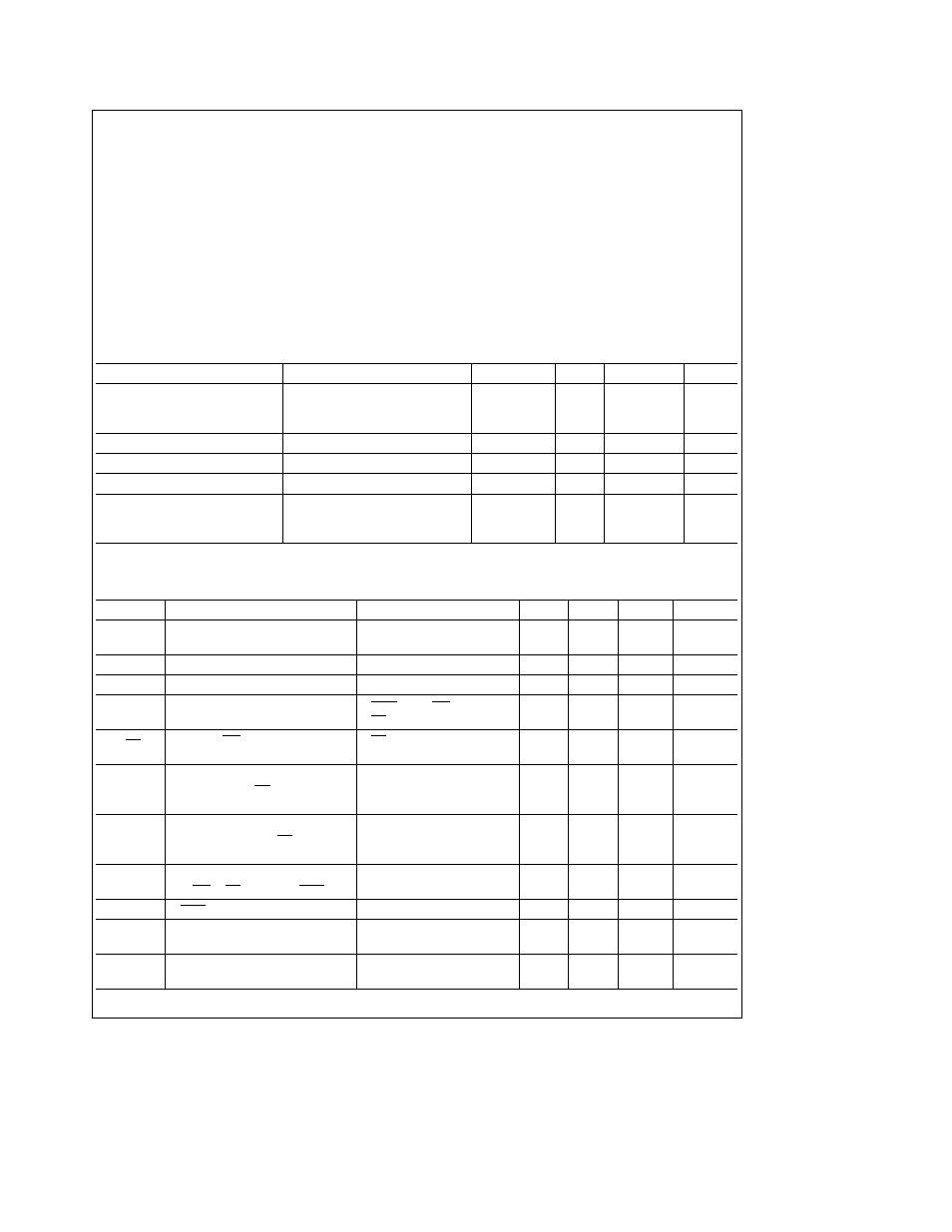
Absolute Maximum Ratings
(Notes 1
2)
If Military Aerospace specified devices are required
please contact the National Semiconductor Sales
Office Distributors for availability and specifications
Supply Voltage (V
CC
) (Note 3)
6 5V
Logic Control Inputs
b
0 3V to a18V
Voltage at Other Inputs and Outputs b0 3V to (V
CC
a
0 3V)
Storage Temperature Range
b
65 C to a150 C
Package Dissipation at T
A
e
25 C
875 mW
Lead Temp (Soldering 10 seconds)
300 C
ESD Susceptibility (Note 10)
800V
Operating Conditions
(Notes 1
2)
Temperature Range
T
MIN
s
T
A
s
T
MAX
ADC1001CCJ
b
40 C
s
T
A
s
a
85 C
ADC1001CCJ-1
0 C
s
T
A
s
a
70 C
Range of V
CC
4 5 V
DC
to 6 3 V
DC
Converter Characteristics
Converter Specifications
V
CC
e
5 V
DC
V
REF
2e2 500 V
DC
T
MIN
s
T
A
s
T
MAX
and f
CLK
e
410 kHz unless otherwise specified
Parameter
Conditions
MIn
Typ
Max
Units
Linearity Error
g
1
LSB
Zero Error
g
2
LSB
Full-Scale Error
g
2
LSB
Total Ladder Resistance (Note 9)
Input Resistance at Pin 9
2 2
4 8
KX
Analog Input Voltage Range
(Note 4) V(a) or V(b)
GNDb0 05
V
CC
a
0 05
V
DC
DC Common-Mode Error
Over Analog Input Voltage Range
g
LSB
Power Supply Sensitivity
V
CC
e
5 V
DC
g
5% Over
g
LSB
Allowed V
IN
(a) and V
IN
(b)
Voltage Range (Note 4)
AC Electrical Characteristics
Timing Specifications
V
CC
e
5 V
DC
and T
A
e
25 C unless otherwise specified
Symbol
Parameter
Conditions
MIn
Typ
Max
Units
T
c
Conversion Time
(Note 5)
80
90
1 f
CLK
f
CLK
e
410 kHz
195
220
m
s
f
CLK
Clock Frequency
(Note 8)
100
1260
kHz
Clock Duty Cycle
40
60
%
CR
Conversion Rate In Free-Running
INTR tied to WR with
4600
conv s
Mode
CSe0 V
DC
f
CLK
e
410 kHz
t
W(WR)L
Width of WR Input (Start Pulse
CSe0 V
DC
(Note 6)
150
ns
Width)
t
ACC
Access Time (Delay from
C
L
e
100 pF
170
300
ns
Falling Edge of RD to Output
Data Valid)
t
1H
t
0H
TRI-STATE Control (Delay
C
L
e
10 pF R
L
e
10k
125
200
ns
from Rising Edge of RD to
(See TRI-STATE Test
Hi-Z State)
Circuits)
t
WI
t
RI
Delay from Falling Edge
300
450
ns
of WR or RD to Reset of INTR
t
1rs
INTR to 1st Read Set-Up Time
550
400
ns
C
IN
Input Capacitance of Logic
5
7 5
pF
Control Inputs
C
OUT
TRI-STATE Output
5
7 5
pF
Capacitance (Data Buffers)
2